|
Stepper
A stepper is a device used in the manufacture of integrated circuits (ICs) that is similar in operation to a slide projector or a photographic enlarger. ''Stepper'' is short for step-and-repeat camera. Steppers are an essential part of the complex process, called photolithography, which creates millions of microscopic circuit elements on the surface of chips of silicon. These chips form the heart of ICs such as computer processors, memory chips, and many other devices. The stepper emerged in the late 1970s but did not become widespread until the 1980s. This was because it was replacing an earlier technology, the mask aligner. Aligners imaged the entire surface of a wafer at the same time, producing many chips in a single operation. In contrast, the stepper imaged only one chip at a time, and was thus much slower to operate. The stepper eventually displaced the aligner when the relentless forces of Moore's Law demanded that smaller feature sizes be used. Because the stepper im ... [...More Info...] [...Related Items...] OR: [Wikipedia] [Google] [Baidu] |
Photomask
A photomask is an opaque plate with holes or transparencies that allow light to shine through in a defined pattern. They are commonly used in photolithography and the production of integrated circuits (ICs or "chips") in particular. Masks are used to produce a pattern on a substrate, normally a thin slice of silicon known as a wafer in the case of chip manufacturing. Several masks are used in turn, each one reproducing a layer of the completed design, and together they are known as a mask set. Previously, photomasks used to be produced manually by using rubylith and mylar. As complexity continued to grow, manual processing of any sort became difficult. This was solved with the introduction of the optical pattern generator which automated the process of producing the initial large-scale pattern, and the step-and-repeat cameras that automated the copying of the pattern into a multiple-IC mask. The intermediate masks are known as reticles, and were initially copied to production mas ... [...More Info...] [...Related Items...] OR: [Wikipedia] [Google] [Baidu] |
Photolithography
In integrated circuit manufacturing, photolithography or optical lithography is a general term used for techniques that use light to produce minutely patterned thin films of suitable materials over a substrate, such as a silicon wafer, to protect selected areas of it during subsequent etching, deposition, or implantation operations. Typically, ultraviolet light is used to transfer a geometric design from an optical mask to a light-sensitive chemical (photoresist) coated on the substrate. The photoresist either breaks down or hardens where it is exposed to light. The patterned film is then created by removing the softer parts of the coating with appropriate solvents. Conventional photoresists typically consists of three components: resin, sensitizer, and solvent. Photolithography processes can be classified according to the type of light used, such as ultraviolet, deep ultraviolet, extreme ultraviolet, or X-ray. The wavelength of light used determines the minimum feature si ... [...More Info...] [...Related Items...] OR: [Wikipedia] [Google] [Baidu] |
Micralign
The Perkin-Elmer Micralign was a family of aligners introduced in 1973. Micralign was the first projection aligner, a concept that dramatically improved semiconductor fabrication. According to the Chip History Center, it "literally made the modern IC industry". The Micralign addressed a significant problem in the early integrated circuit (IC) industry, that the vast majority of ICs printed contained defects that rendered them useless. On average, about 1 in 10 complex ICs produced would be operational, a 10% yield. The Micralign improved this to over 50%, and as great as 70% in many applications. In doing so, the price of microprocessors and dynamic RAM products fell about 10 times between 1974 and 1978, by which time the Micralign had become practically universal in the high-end market. Initially predicting to sell perhaps 50 units, Perkin-Elmer eventually sold about 2,000, making them the by far largest vendor in the semiconductor fabrication equipment space through the second h ... [...More Info...] [...Related Items...] OR: [Wikipedia] [Google] [Baidu] |
Perkin-Elmer
PerkinElmer, Inc., previously styled Perkin-Elmer, is an American global corporation focused in the business areas of diagnostics, life science research, food, environmental and industrial testing. Its capabilities include detection, imaging, informatics, and service. PerkinElmer produces analytical instruments, genetic testing and diagnostic tools, medical imaging components, software, instruments, and consumables for multiple end markets. PerkinElmer is part of the S&P 500 Index and operates in 190 countries. History Founding Richard Scott Perkin, Richard Perkin was attending the Pratt Institute in Brooklyn to study chemical engineering, but left after a year to try his hand on Wall Street. Still interested in the sciences, he gave public lectures on various topics. Charles Wesley Elmer, Charles Elmer ran a firm that supplied court reporters and was nearing retirement when he attended one of Perkin's lectures on astronomy being held at the Brooklyn Institute of Arts and Sci ... [...More Info...] [...Related Items...] OR: [Wikipedia] [Google] [Baidu] |
ASM International
ASM International is a Dutch headquartered multinational corporation that specializes in design, manufacturing, sales and service of semiconductor wafer processing equipment for the fabrication of semiconductor devices. ASM's products are used by semiconductor manufacturers in front-end wafer processing in their semiconductor fabrication plants. ASM’s technologies include atomic layer deposition, epitaxy, chemical vapor deposition and diffusion. The company was founded by Arthur del Prado (1931-2016) as ‘Advanced Semiconductor Materials’ in 1964. From 2008 until 2020, son of Arthur del Prado, Chuck del Prado was CEO. ASM pioneered important aspects of many established wafer-processing technologies used in industry, including lithography, deposition, ion implantation, single-wafer epitaxy, and in recent years atomic layer deposition. Semiconductor equipment companies ASML, ASM Pacific Technology and Besi are former divisions of ASM. ASM International headq ... [...More Info...] [...Related Items...] OR: [Wikipedia] [Google] [Baidu] |
Wafer (electronics)
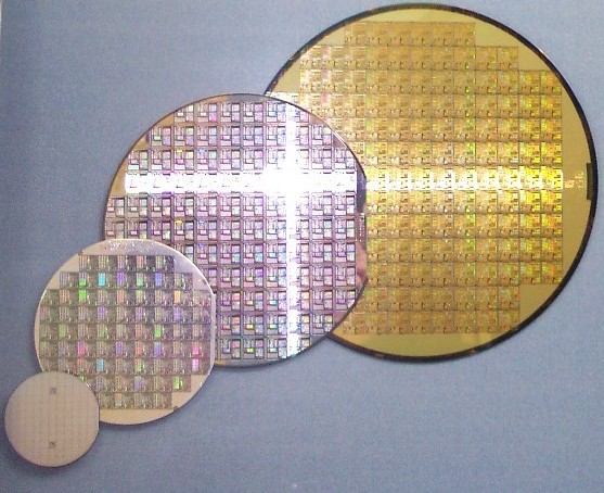
In electronics, a wafer (also called a slice or substrate) is a thin slice of semiconductor, such as a crystalline silicon Crystalline silicon or (c-Si) Is the crystalline forms of silicon, either polycrystalline silicon (poly-Si, consisting of small crystals), or monocrystalline silicon (mono-Si, a continuous crystal). Crystalline silicon is the dominant semiconduc ... (c-Si), used for the fabrication of integrated circuits and, in photovoltaics, to manufacture solar cells. The wafer serves as the substrate (materials science), substrate for microelectronic devices built in and upon the wafer. It undergoes many microfabrication processes, such as doping (semiconductor), doping, ion implantation, Etching (microfabrication), etching, thin-film deposition of various materials, and Photolithography, photolithographic patterning. Finally, the individual microcircuits are separated by wafer dicing and Integrated circuit packaging, packaged as an integrated circuit. History I ... [...More Info...] [...Related Items...] OR: [Wikipedia] [Google] [Baidu] |
Microscope
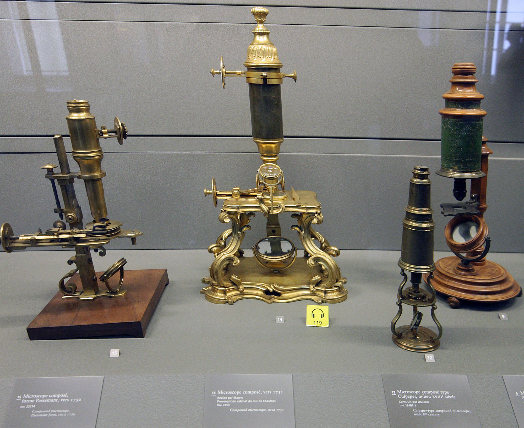
A microscope () is a laboratory instrument used to examine objects that are too small to be seen by the naked eye. Microscopy is the science of investigating small objects and structures using a microscope. Microscopic means being invisible to the eye unless aided by a microscope. There are many types of microscopes, and they may be grouped in different ways. One way is to describe the method an instrument uses to interact with a sample and produce images, either by sending a beam of light or electrons through a sample in its optical path, by detecting photon emissions from a sample, or by scanning across and a short distance from the surface of a sample using a probe. The most common microscope (and the first to be invented) is the optical microscope, which uses lenses to refract visible light that passed through a thinly sectioned sample to produce an observable image. Other major types of microscopes are the fluorescence microscope, electron microscope (both the transmi ... [...More Info...] [...Related Items...] OR: [Wikipedia] [Google] [Baidu] |
Solvent
A solvent (s) (from the Latin '' solvō'', "loosen, untie, solve") is a substance that dissolves a solute, resulting in a solution. A solvent is usually a liquid but can also be a solid, a gas, or a supercritical fluid. Water is a solvent for polar molecules and the most common solvent used by living things; all the ions and proteins in a cell are dissolved in water within the cell. The quantity of solute that can dissolve in a specific volume of solvent varies with temperature. Major uses of solvents are in paints, paint removers, inks, and dry cleaning. Specific uses for organic solvents are in dry cleaning (e.g. tetrachloroethylene); as paint thinners (toluene, turpentine); as nail polish removers and solvents of glue (acetone, methyl acetate, ethyl acetate); in spot removers (hexane, petrol ether); in detergents ( citrus terpenes); and in perfumes (ethanol). Solvents find various applications in chemical, pharmaceutical, oil, and gas industries, including in chemical syn ... [...More Info...] [...Related Items...] OR: [Wikipedia] [Google] [Baidu] |
Ultraviolet
Ultraviolet (UV) is a form of electromagnetic radiation with wavelength from 10 nanometer, nm (with a corresponding frequency around 30 Hertz, PHz) to 400 nm (750 Hertz, THz), shorter than that of visible light, but longer than X-rays. UV radiation is present in sunlight, and constitutes about 10% of the total electromagnetic radiation output from the Sun. It is also produced by electric arcs and specialized lights, such as mercury-vapor lamps, tanning lamps, and black lights. Although long-wavelength ultraviolet is not considered an ionizing radiation because its photons lack the energy to ionization, ionize atoms, it can cause chemical reactions and causes many substances to glow or fluorescence, fluoresce. Consequently, the chemical and biological effects of UV are greater than simple heating effects, and many practical applications of UV radiation derive from its interactions with organic molecules. Short-wave ultraviolet light damages DNA and sterilizes surf ... [...More Info...] [...Related Items...] OR: [Wikipedia] [Google] [Baidu] |
Photoresist
A photoresist (also known simply as a resist) is a light-sensitive material used in several processes, such as photolithography and photoengraving, to form a patterned coating on a surface. This process is crucial in the electronic industry. The process begins by coating a substrate with a light-sensitive organic material. A patterned mask is then applied to the surface to block light, so that only unmasked regions of the material will be exposed to light. A solvent, called a developer, is then applied to the surface. In the case of a positive photoresist, the photo-sensitive material is degraded by light and the developer will dissolve away the regions that were exposed to light, leaving behind a coating where the mask was placed. In the case of a negative photoresist, the photosensitive material is strengthened (either polymerized or cross-linked) by light, and the developer will dissolve away only the regions that were not exposed to light, leaving behind a coating in areas w ... [...More Info...] [...Related Items...] OR: [Wikipedia] [Google] [Baidu] |
Silicon Wafer
In electronics, a wafer (also called a slice or substrate) is a thin slice of semiconductor, such as a crystalline silicon (c-Si), used for the fabrication of integrated circuits and, in photovoltaics, to manufacture solar cells. The wafer serves as the substrate for microelectronic devices built in and upon the wafer. It undergoes many microfabrication processes, such as doping, ion implantation, etching, thin-film deposition of various materials, and photolithographic patterning. Finally, the individual microcircuits are separated by wafer dicing and packaged as an integrated circuit. History In the semiconductor or silicon wafer industry, the term wafer appeared in the 1950s to describe a thin round slice of semiconductor material, typically germanium or silicon. Round shape comes from single-crystal ingots usually produced using the Czochralski method. Silicon wafers were first introduced in the 1940s. By 1960, silicon wafers were being manufactured in the U.S. by ... [...More Info...] [...Related Items...] OR: [Wikipedia] [Google] [Baidu] |


