|
IGFET
The metal–oxide–semiconductor field-effect transistor (MOSFET, MOS-FET, or MOS FET) is a type of field-effect transistor (FET), most commonly fabricated by the controlled oxidation of silicon. It has an insulated gate, the voltage of which determines the conductivity of the device. This ability to change conductivity with the amount of applied voltage can be used for amplifying or switching electronic signals. A metal-insulator-semiconductor field-effect transistor (MISFET) is a term almost synonymous with MOSFET. Another synonym is IGFET for insulated-gate field-effect transistor. The basic principle of the field-effect transistor was first patented by Julius Edgar Lilienfeld in 1925.Lilienfeld, Julius Edgar (1926-10-08) "Method and apparatus for controlling electric currents" upright=1.6, Two power MOSFETs in V_in_the_''off''_state,_and_can_conduct_a_continuous_current_of_30 surface-mount_packages._Operating_as_switches,_each_of_these_components_can_sust ... [...More Info...] [...Related Items...] OR: [Wikipedia] [Google] [Baidu] |
Transistor
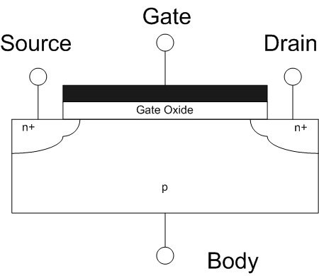
upright=1.4, gate (G), body (B), source (S) and drain (D) terminals. The gate is separated from the body by an insulating layer (pink). A transistor is a semiconductor device used to Electronic amplifier, amplify or electronic switch, switch electrical signals and electrical power, power. The transistor is one of the basic building blocks of modern electronics. It is composed of semiconductor material, usually with at least three terminals for connection to an electronic circuit. A voltage or current applied to one pair of the transistor's terminals controls the current through another pair of terminals. Because the controlled (output) power can be higher than the controlling (input) power, a transistor can amplify a signal. Some transistors are packaged individually, but many more are found embedded in integrated circuits. Austro-Hungarian physicist Julius Edgar Lilienfeld proposed the concept of a field-effect transistor in 1926, but it was not possible to actually constru ... [...More Info...] [...Related Items...] OR: [Wikipedia] [Google] [Baidu] |
MOSFET Structure
The metal–oxide–semiconductor field-effect transistor (MOSFET, MOS-FET, or MOS FET) is a type of field-effect transistor (FET), most commonly fabricated by the controlled oxidation of silicon. It has an insulated gate, the voltage of which determines the conductivity of the device. This ability to change conductivity with the amount of applied voltage can be used for amplifying or switching electronic signals. A metal-insulator-semiconductor field-effect transistor (MISFET) is a term almost synonymous with MOSFET. Another synonym is IGFET for insulated-gate field-effect transistor. The basic principle of the field-effect transistor was first patented by Julius Edgar Lilienfeld in 1925.Lilienfeld, Julius Edgar (1926-10-08) "Method and apparatus for controlling electric currents" upright=1.6, Two power MOSFETs in V_in_the_''off''_state,_and_can_conduct_a_continuous_current_of_30 surface-mount_packages._Operating_as_switches,_each_of_these_components_can_sus ... [...More Info...] [...Related Items...] OR: [Wikipedia] [Google] [Baidu] |
MOSFET Functioning Body
The metal–oxide–semiconductor field-effect transistor (MOSFET, MOS-FET, or MOS FET) is a type of field-effect transistor (FET), most commonly fabricated by the controlled oxidation of silicon. It has an insulated gate, the voltage of which determines the conductivity of the device. This ability to change conductivity with the amount of applied voltage can be used for amplifying or switching electronic signals. A metal-insulator-semiconductor field-effect transistor (MISFET) is a term almost synonymous with MOSFET. Another synonym is IGFET for insulated-gate field-effect transistor. The basic principle of the field-effect transistor was first patented by Julius Edgar Lilienfeld in 1925.Lilienfeld, Julius Edgar (1926-10-08) "Method and apparatus for controlling electric currents" upright=1.6, Two power MOSFETs in V_in_the_''off''_state,_and_can_conduct_a_continuous_current_of_30 surface-mount_packages._Operating_as_switches,_each_of_these_components_can_sus ... [...More Info...] [...Related Items...] OR: [Wikipedia] [Google] [Baidu] |
MOSFETs
The metal–oxide–semiconductor field-effect transistor (MOSFET, MOS-FET, or MOS FET) is a type of field-effect transistor (FET), most commonly fabricated by the controlled oxidation of silicon. It has an insulated gate, the voltage of which determines the conductivity of the device. This ability to change conductivity with the amount of applied voltage can be used for amplifying or switching electronic signals. A metal-insulator-semiconductor field-effect transistor (MISFET) is a term almost synonymous with MOSFET. Another synonym is IGFET for insulated-gate field-effect transistor. The basic principle of the field-effect transistor was first patented by Julius Edgar Lilienfeld in 1925.Lilienfeld, Julius Edgar (1926-10-08) "Method and apparatus for controlling electric currents" upright=1.6, Two power MOSFETs in V_in_the_''off''_state,_and_can_conduct_a_continuous_current_of_30 surface-mount_packages._Operating_as_switches,_each_of_these_components_can_sus ... [...More Info...] [...Related Items...] OR: [Wikipedia] [Google] [Baidu] |
MOS Capacitor
The metal–oxide–semiconductor field-effect transistor (MOSFET, MOS-FET, or MOS FET) is a type of field-effect transistor (FET), most commonly fabricated by the controlled oxidation of silicon. It has an insulated gate, the voltage of which determines the conductivity of the device. This ability to change conductivity with the amount of applied voltage can be used for amplifying or switching electronic signals. A metal-insulator-semiconductor field-effect transistor (MISFET) is a term almost synonymous with MOSFET. Another synonym is IGFET for insulated-gate field-effect transistor. The basic principle of the field-effect transistor was first patented by Julius Edgar Lilienfeld in 1925.Lilienfeld, Julius Edgar (1926-10-08) "Method and apparatus for controlling electric currents" upright=1.6, Two power MOSFETs in V_in_the_''off''_state,_and_can_conduct_a_continuous_current_of_30 surface-mount_packages._Operating_as_switches,_each_of_these_components_can_sus ... [...More Info...] [...Related Items...] OR: [Wikipedia] [Google] [Baidu] |
Field-effect Transistor
The field-effect transistor (FET) is a type of transistor that uses an electric field to control the flow of current in a semiconductor. FETs (JFETs or MOSFETs) are devices with three terminals: ''source'', ''gate'', and ''drain''. FETs control the flow of current by the application of a voltage to the gate, which in turn alters the conductivity between the drain and source. FETs are also known as unipolar transistors since they involve single-carrier-type operation. That is, FETs use either electrons (n-channel) or holes (p-channel) as charge carriers in their operation, but not both. Many different types of field effect transistors exist. Field effect transistors generally display very high input impedance at low frequencies. The most widely used field-effect transistor is the MOSFET (metal-oxide-semiconductor field-effect transistor). History The concept of a field-effect transistor (FET) was first patented by Austro-Hungarian physicist Julius Edgar Lilienfeld in 192 ... [...More Info...] [...Related Items...] OR: [Wikipedia] [Google] [Baidu] |
Julius Edgar Lilienfeld
Julius Edgar Lilienfeld (April 18, 1882 – August 28, 1963) was an Austro-Hungarian, and later American (where he moved in 1921) physicist and electrical engineer, who was credited with the first patent on the field-effect (FET) (1925). Because of his failure to publish articles in learned journals and because high-purity semiconductor materials were not available yet, his FET patent never achieved fame, causing confusion for later inventors. Early life Lilienfeld was born into a German-speaking Ashkenazi Jewish family in Lemberg (present-day Lviv) in the Austrian part of the Austro-Hungarian Empire. Education Between 1900 and 1904, Lilienfeld studied at the Friedrich-Wilhelms-Universität (renamed Humboldt University in 1949), in Berlin, where he received his Ph.D. on February 18, 1905. In 1905, he started work at the physics institute at Leipzig University as an untenured professor. Career Lilienfeld's early career, at the University of Leipzig, saw him conduct impor ... [...More Info...] [...Related Items...] OR: [Wikipedia] [Google] [Baidu] |
Integrated Circuit
An integrated circuit or monolithic integrated circuit (also referred to as an IC, a chip, or a microchip) is a set of electronic circuits on one small flat piece (or "chip") of semiconductor material, usually silicon. Large numbers of tiny MOSFETs (metal–oxide–semiconductor field-effect transistors) integrate into a small chip. This results in circuits that are orders of magnitude smaller, faster, and less expensive than those constructed of discrete electronic components. The IC's mass production capability, reliability, and building-block approach to integrated circuit design has ensured the rapid adoption of standardized ICs in place of designs using discrete transistors. ICs are now used in virtually all electronic equipment and have revolutionized the world of electronics. Computers, mobile phones and other home appliances are now inextricable parts of the structure of modern societies, made possible by the small size and low cost of ICs such as modern computer ... [...More Info...] [...Related Items...] OR: [Wikipedia] [Google] [Baidu] |
Electrical Conductivity
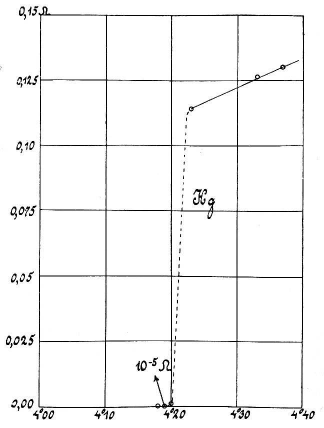
Electrical resistivity (also called specific electrical resistance or volume resistivity) is a fundamental property of a material that measures how strongly it resists electric current. A low resistivity indicates a material that readily allows electric current. Resistivity is commonly represented by the Greek letter (rho). The SI unit of electrical resistivity is the ohm-meter (Ω⋅m). For example, if a solid cube of material has sheet contacts on two opposite faces, and the resistance between these contacts is , then the resistivity of the material is . Electrical conductivity or specific conductance is the reciprocal of electrical resistivity. It represents a material's ability to conduct electric current. It is commonly signified by the Greek letter ( sigma), but ( kappa) (especially in electrical engineering) and ( gamma) are sometimes used. The SI unit of electrical conductivity is siemens per metre (S/m). Resistivity and conductivity are inte ... [...More Info...] [...Related Items...] OR: [Wikipedia] [Google] [Baidu] |
45 Nanometer
Per the International Technology Roadmap for Semiconductors, the 45 nm process is a MOSFET technology node referring to the average half-pitch of a memory cell manufactured at around the 2007–2008 time frame. Matsushita and Intel started mass-producing 45 nm chips in late 2007, and AMD started production of 45 nm chips in late 2008, while IBM, Infineon, Samsung, and Chartered Semiconductor have already completed a common 45 nm process platform. At the end of 2008, SMIC was the first China-based semiconductor company to move to 45 nm, having licensed the bulk 45 nm process from IBM. In 2008, TSMC moved on to a 40nm process. Many critical feature sizes are smaller than the wavelength of light used for lithography (i.e., 193 nm and 248 nm). A variety of techniques, such as larger lenses, are used to make sub-wavelength features. Double patterning has also been introduced to assist in shrinking distances between features, especially if dry lit ... [...More Info...] [...Related Items...] OR: [Wikipedia] [Google] [Baidu] |
Silicon Oxynitride
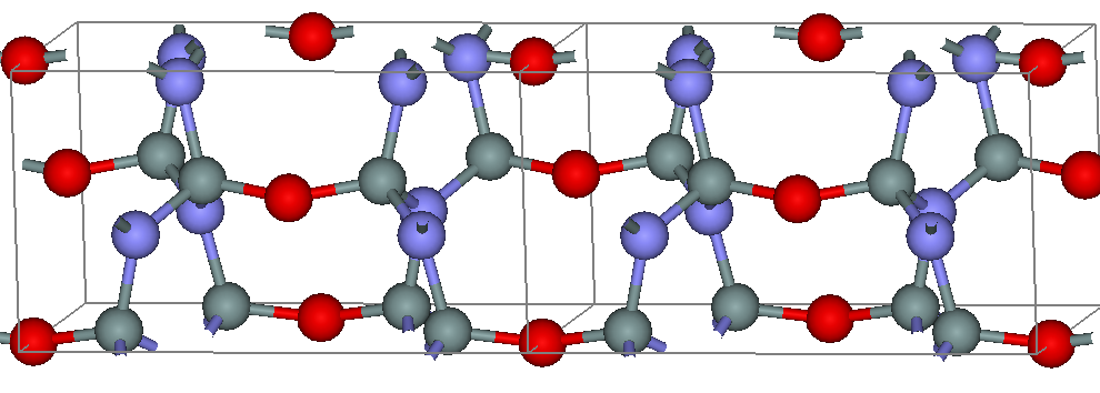
Silicon oxynitride is a ceramic material with the chemical formula SiOxNy. While in amorphous forms its composition can continuously vary between SiO2 (silica) and Si3N4 (silicon nitride), the only known intermediate crystalline phase is Si2N2O. It is found in nature as the rare mineral sinoite in some meteorites and can be synthesized in the laboratory. Properties The crystalline structure of silicon oxynitride is built by SiN3O tetrahedra connected through oxygen atoms along the ''c'' axis and through nitrogen atoms perpendicular to it. The strong covalent bonding of this structure results in high flexural strength and resistance to heating and oxidation up to temperatures of about 1600 °C. Synthesis Polycrystalline silicon oxynitride ceramics are primarily produced by nitridation of a mixture of Si and silicon dioxide at a temperature above melting point of silicon (1414 °C), in the range 1420–1500 °C: :3 Si + SiO2 + 2 N2 → 2 Si2N2O Silicon oxynitride ma ... [...More Info...] [...Related Items...] OR: [Wikipedia] [Google] [Baidu] |
High-κ Dielectric
The term high-κ dielectric refers to a material with a high dielectric constant (κ, kappa), as compared to silicon dioxide. High-κ dielectrics are used in semiconductor manufacturing processes where they are usually used to replace a silicon dioxide gate dielectric or another dielectric layer of a device. The implementation of high-κ gate dielectrics is one of several strategies developed to allow further miniaturization of microelectronic components, colloquially referred to as extending Moore's Law. Sometimes these materials are called "high-k" (pronounced "high kay"), instead of "high-κ" (high kappa). Need for high-κ materials Silicon dioxide () has been used as a gate oxide material for decades. As metal-oxide-semiconductor field-effect transistors (MOSFETs) have decreased in size, the thickness of the silicon dioxide gate dielectric has steadily decreased to increase the gate capacitance (per unit area) and thereby drive current (per device width), raising device perfor ... [...More Info...] [...Related Items...] OR: [Wikipedia] [Google] [Baidu] |
.jpg)

.jpg)

