|
Technology CAD
Technology computer-aided design (technology CAD or TCAD) is a branch of electronic design automation that models semiconductor fabrication and semiconductor device operation. The modeling of the fabrication is termed Process TCAD, while the modeling of the device operation is termed Device TCAD. Included are the modelling of process steps (such as diffusion and ion implantation), and modelling of the behavior of the electrical devices based on fundamental physics, such as the doping profiles of the devices. TCAD may also include the creation of ''compact models'' (such as the well known SPICE transistor models), which try to capture the electrical behavior of such devices but do not generally derive them from the underlying physics. SPICE simulator itself is usually considered as part of ECAD rather than TCAD. Introduction Technology files and design rules are essential building blocks of the integrated circuit design process. Their accuracy and robustness over process tec ... [...More Info...] [...Related Items...] OR: [Wikipedia] [Google] [Baidu] |
Latchup
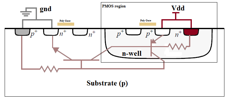
A latch-up is a type of short circuit which can occur in an integrated circuit (IC). More specifically it is the inadvertent creation of a low- impedance path between the power supply rails of a MOSFET circuit, triggering a parasitic structure which disrupts proper functioning of the part, possibly even leading to its destruction due to overcurrent. A power cycle is required to correct this situation. The parasitic structure is usually equivalent to a thyristor (or SCR), a PNPN structure which acts as a PNP and an NPN transistor stacked next to each other. During a latch-up when one of the transistors is conducting, the other one begins conducting too. They both keep each other in saturation for as long as the structure is forward-biased and some current flows through it - which usually means until a power-down. The SCR parasitic structure is formed as a part of the totem-pole PMOS and NMOS transistor pair on the output drivers of the gates. The latch-up does not have to happen ... [...More Info...] [...Related Items...] OR: [Wikipedia] [Google] [Baidu] |
Crosslight Software
Crosslight Software Inc. is an international company headquartered in greater Vancouver, British Columbia, Canada. Officially spun off from the National Research Council of Canada (NRC) in 1995, it provides Technology Computer Aided Design ( TCAD) tools for semiconductor device and process simulations. Crosslight's founder, Dr. Z.M. Simon Li (李湛明), is a pioneer in the field of optoelectronic device simulation TCAD and based on this work, Crosslight claims to be the first commercial vendor of TCAD tools for quantum well laser diodes. Crosslight also licenses other technology from the Stanford UniversityTCAD Groupfor semiconductor process simulations. History After its initial spin-off from the NRC, Crosslight launched its flagship product LASTIP, a 2D simulator for quantum well laser diodes. Based on its founder's research, LASTIP predates other well-known tools in the field such as MINILASE. By adding the ability to model quantum well active regions, LASTIP was al ... [...More Info...] [...Related Items...] OR: [Wikipedia] [Google] [Baidu] |
Silvaco
Silvaco Group, Inc., develops and markets electronic design automation (EDA) and technology CAD (TCAD) software and semiconductor design IP (SIP). The company is headquartered in Santa Clara, California, and has a global presence with offices located in North America, Europe, and throughout Asia. Since its founding in 1984, Silvaco has grown to become a large privately held EDA company. The company has been known by at least two other names: Silvaco International, and Silvaco Data Systems. History Founded by Dr. Ivan Pesic (13 September 1951, Resnik, Montenegro — 20 October 2012, Japan) in 1984, the company is privately held and internally funded. It is headquartered in Santa Clara, California, with fourteen offices worldwide. In 2003 Silvaco acquired Simucad Inc., a privately held company founded in 1981 that provided logic simulation EDA software. Silvaco re-launched the brand by spinning out its EDA product line in 2006 under the Simucad name. As of 17 February 2010, ... [...More Info...] [...Related Items...] OR: [Wikipedia] [Google] [Baidu] |
Synopsys
Synopsys is an American electronic design automation (EDA) company that focuses on silicon design and verification, silicon intellectual property and software security and quality. Products include tools for logic synthesis and physical design of integrated circuits, simulators for development and debugging environments that assist in the design of the logic for chips and computer systems. In recent years, Synopsys has expanded its products and services to include application security testing. Synopsys has gained attention due to its relationship with various Chinese state entities. In 2018, Synopsys formed a partnership with the People's Liberation Army National Defence University and, in 2022, the company came under investigation by the United States Department of Justice for technology transfers to sanctioned entities in China. History Synopsys was founded by Aart J de Geus and David Gregory in 1986 in Research Triangle Park, North Carolina. The company was initially est ... [...More Info...] [...Related Items...] OR: [Wikipedia] [Google] [Baidu] |
BACPAC
BACPAC, or the Berkeley Advanced Chip Performance Calculator, is a software program to explore the effect of changes in IC technology. The use enters a set of fairly fundamental properties of the technology (such as interconnect layer thickness, and logic depth) and the program estimates the system level performance of an IC built with these assumptions. Previous work in this area can be found in and, but these do not consider many of the effects of deep-sub-micrometre interconnect. BACPAC is based on the work in.D. Sylvester and K. Keutzer, “Getting to the bottom of deep submicron,” Proc. of International Conference on CAD, pp. 203–211, 1998. BACPAC uses analytical approximations for system properties such as delay and interconnect requirements. The intent is not absolute accuracy for a given design, but to show trends and effects of technology changes. Inputs to BACPAC Interconnect *Number of routing layers *Pitches (center to center distance of each layer) *Res ... [...More Info...] [...Related Items...] OR: [Wikipedia] [Google] [Baidu] |
Semiconductor Process Simulation
Semiconductor process simulation is the modeling of the fabrication of semiconductor devices such as transistors. It is a branch of electronic design automation, and part of a sub-field known as technology CAD, or TCAD. This summary was derived (with permission) from Vol I, Chapter 24, Process Simulation, by Mark Johnson. The ultimate goal of process simulation is an accurate prediction of the active dopant distribution, the stress distribution and the device geometry. Process simulation is typically used as an input for device simulation, the modeling of device electrical characteristics. Collectively process and device simulation form the core tools for the design phase known as TCAD or Technology Computer Aided Design. Considering the integrated circuit design process as a series of steps with decreasing levels of abstraction, logic synthesis would be at the highest level and TCAD, being closest to fabrication, would be the phase with the least amount of abstraction. ... [...More Info...] [...Related Items...] OR: [Wikipedia] [Google] [Baidu] |
Doping (semiconductor)
In semiconductor production, doping is the intentional introduction of impurities into an intrinsic semiconductor for the purpose of modulating its electrical, optical and structural properties. The doped material is referred to as an extrinsic semiconductor. Small numbers of dopant atoms can change the ability of a semiconductor to conduct electricity. When on the order of one dopant atom is added per 100 million atoms, the doping is said to be ''low'' or ''light''. When many more dopant atoms are added, on the order of one per ten thousand atoms, the doping is referred to as ''high'' or ''heavy''. This is often shown as ''n+'' for n-type doping or ''p+'' for p-type doping. (''See the article on semiconductors for a more detailed description of the doping mechanism.'') A semiconductor doped to such high levels that it acts more like a conductor than a semiconductor is referred to as a degenerate semiconductor. A semiconductor can be considered i-type semiconductor if it has ... [...More Info...] [...Related Items...] OR: [Wikipedia] [Google] [Baidu] |
Hardware Description Language
In computer engineering, a hardware description language (HDL) is a specialized computer language used to describe the structure and behavior of electronic circuits, and most commonly, digital logic circuits. A hardware description language enables a precise, formal description of an electronic circuit that allows for the automated analysis and simulation of an electronic circuit. It also allows for the synthesis of an HDL description into a netlist (a specification of physical electronic components and how they are connected together), which can then be placed and routed to produce the set of masks used to create an integrated circuit. A hardware description language looks much like a programming language such as C or ALGOL; it is a textual description consisting of expressions, statements and control structures. One important difference between most programming languages and HDLs is that HDLs explicitly include the notion of time. HDLs form an integral part of electr ... [...More Info...] [...Related Items...] OR: [Wikipedia] [Google] [Baidu] |
Integrated Circuit Design
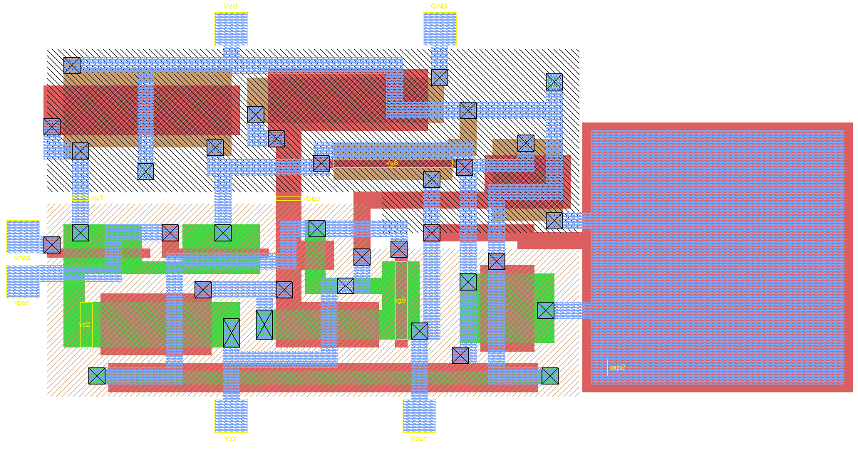
Integrated circuit design, or IC design, is a sub-field of electronics engineering, encompassing the particular logic and circuit design techniques required to design integrated circuits, or ICs. ICs consist of miniaturized electronic components built into an electrical network on a monolithic semiconductor substrate by photolithography. IC design can be divided into the broad categories of digital and analog IC design. Digital IC design is to produce components such as microprocessors, FPGAs, memories (RAM, ROM, and flash) and digital ASICs. Digital design focuses on logical correctness, maximizing circuit density, and placing circuits so that clock and timing signals are routed efficiently. Analog IC design also has specializations in power IC design and RF IC design. Analog IC design is used in the design of op-amps, linear regulators, phase locked loops, oscillators and active filters. Analog design is more concerned with the physics of the semiconductor devices such as ... [...More Info...] [...Related Items...] OR: [Wikipedia] [Google] [Baidu] |
Electromagnetic Field Solver
Electromagnetic field solvers (or sometimes just field solvers) are specialized programs that solve (a subset of) Maxwell's equations directly. They form a part of the field of electronic design automation, or EDA, and are commonly used in the design of integrated circuits and printed circuit boards. They are used when a solution from first principles is needed, or the highest accuracy is required. Introduction The extraction of parasitic circuit models is important for various aspects of physical verification such as timing, signal integrity, substrate coupling, and power grid analysis. As circuit speeds and densities have increased, the need has grown to account accurately for parasitic effects for larger and more complicated interconnect structures. In addition, the electromagnetic complexity has grown as well, from resistance and capacitance, to inductance, and now even full electromagnetic wave propagation. This increase in complexity has also grown for the analy ... [...More Info...] [...Related Items...] OR: [Wikipedia] [Google] [Baidu] |
Chemical-mechanical Planarization
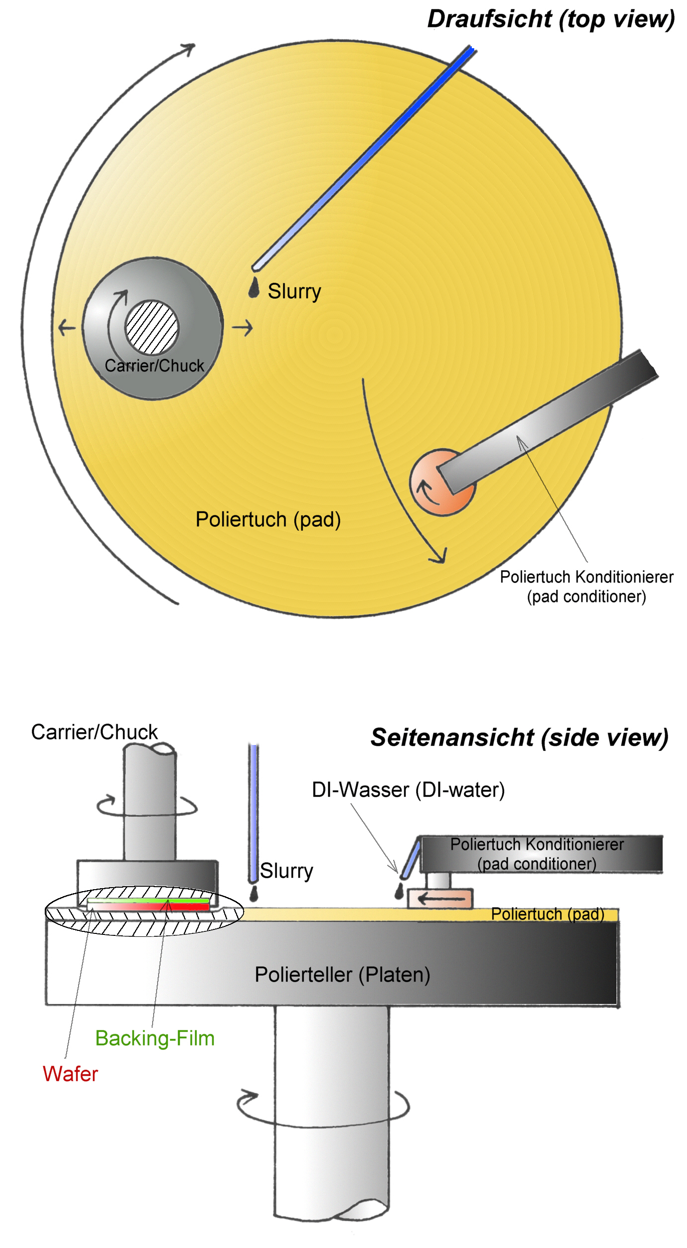
Chemical mechanical polishing (CMP) or planarization is a process of smoothing surfaces with the combination of chemical and mechanical forces. It can be thought of as a hybrid of chemical etching and free abrasive polishing. Description The process uses an abrasive and corrosive chemical slurry (commonly a colloid) in conjunction with a polishing pad and retaining ring, typically of a greater diameter than the wafer. The pad and wafer are pressed together by a dynamic polishing head and held in place by a plastic retaining ring. The dynamic polishing head is rotated with different axes of rotation (i.e., not concentric). This removes material and tends to even out any irregular topography, making the wafer flat or planar. This may be necessary to set up the wafer for the formation of additional circuit elements. For example, CMP can bring the entire surface within the depth of field of a photolithography system, or selectively remove material based on its position. Typical depth-o ... [...More Info...] [...Related Items...] OR: [Wikipedia] [Google] [Baidu] |


