|
Mask Data Preparation
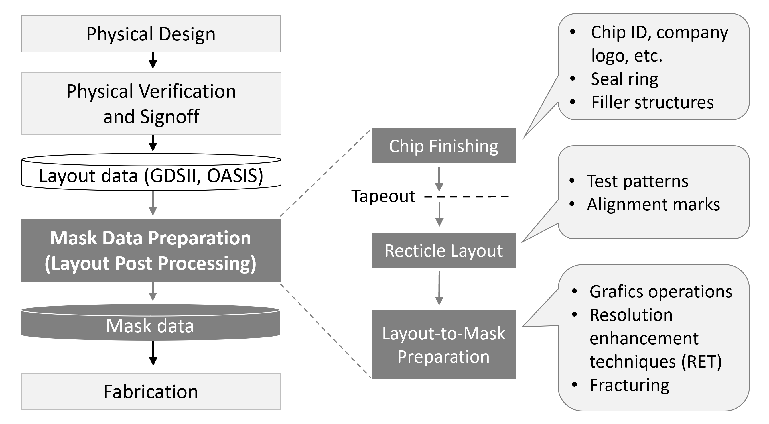
Mask data preparation (MDP), also known as layout post processing, is the procedure of translating a file containing the intended set of polygons from an integrated circuit layout into set of instructions that a photomask writer can use to generate a physical mask. Typically, amendments and additions to the chip layout are performed in order to convert the physical layout into data for mask production. Mask data preparation requires an input file which is in a GDSII or OASIS format, and produces a file that is in a proprietary format specific to the mask writer. MDP procedures Although historically converting the physical layout into data for mask production was relatively simple, more recent MDP procedures require various procedures: * ''Chip finishing'' which includes custom designations and structures to improve manufacturability of the layout. Examples of the latter are a seal ring and filler structures. * Producing a ''reticle layout'' with test patterns and alignment ... [...More Info...] [...Related Items...] OR: [Wikipedia] [Google] [Baidu] |
Integrated Circuit Layout
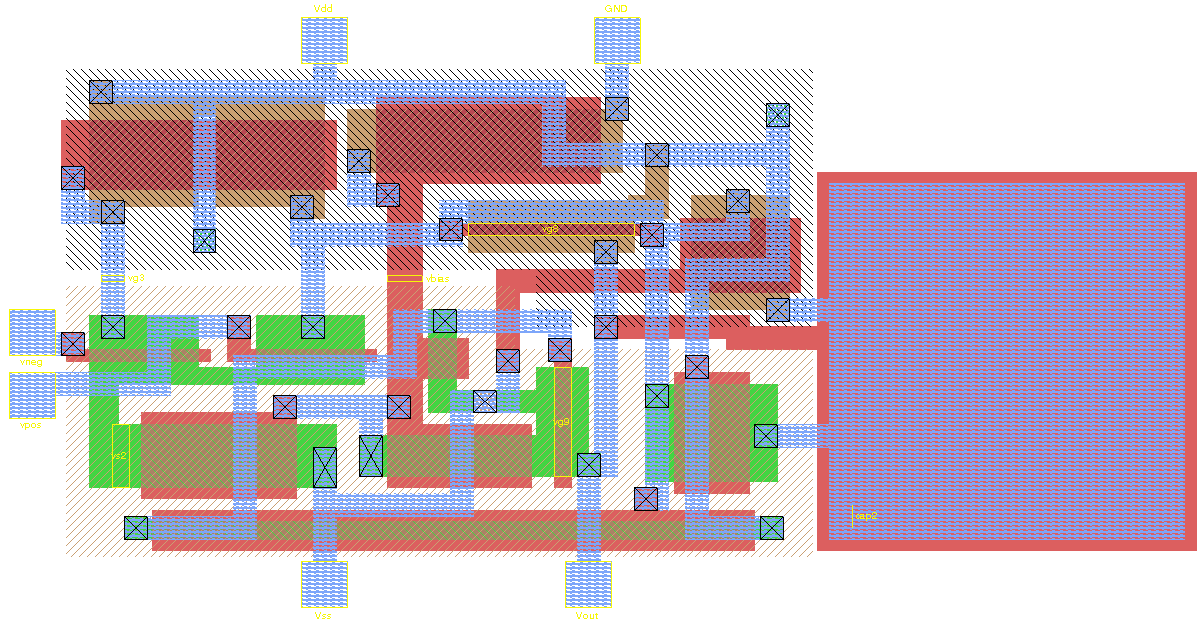
Integrated circuit layout, also known IC layout, IC mask layout, or mask design, is the representation of an integrated circuit in terms of planar geometric shapes which correspond to the patterns of metal, oxide, or semiconductor layers that make up the components of the integrated circuit. Originally the overall process was called tapeout as historically early ICs used graphical black crepe tape on mylar media for photo imaging (erroneously believed to reference magnetic data—the photo process greatly predated magnetic media). When using a standard process—where the interaction of the many chemical, thermal, and photographic variables is known and carefully controlled—the behaviour of the final integrated circuit depends largely on the positions and interconnections of the geometric shapes. Using a computer-aided layout tool, the layout engineer—or layout technician—places and connects all of the components that make up the chip such that they meet certain criteria� ... [...More Info...] [...Related Items...] OR: [Wikipedia] [Google] [Baidu] |
Photomask
A photomask is an opaque plate with holes or transparencies that allow light to shine through in a defined pattern. They are commonly used in photolithography and the production of integrated circuits (ICs or "chips") in particular. Masks are used to produce a pattern on a substrate, normally a thin slice of silicon known as a wafer in the case of chip manufacturing. Several masks are used in turn, each one reproducing a layer of the completed design, and together they are known as a mask set. Previously, photomasks used to be produced manually by using rubylith and mylar. As complexity continued to grow, manual processing of any sort became difficult. This was solved with the introduction of the optical pattern generator which automated the process of producing the initial large-scale pattern, and the step-and-repeat cameras that automated the copying of the pattern into a multiple-IC mask. The intermediate masks are known as reticles, and were initially copied to production mas ... [...More Info...] [...Related Items...] OR: [Wikipedia] [Google] [Baidu] |
GDSII
GDSII stream format (GDSII), is a binary database file format which is the de facto industry standard for Electronic Design Automation data exchange of integrated circuit or IC layout artwork. It is a binary file format representing planar geometric shapes, text labels, and other information about the layout in hierarchical form. The data can be used to reconstruct all or part of the artwork to be used in sharing layouts, transferring artwork between different tools, or creating photomasks. History GDS = Graphic Design System (see DS78 Initially, GDSII was designed as a stream format used to control integrated circuit photomask plotting. Despite its limited set of features and low data density, it became the industry conventional stream format for transfer of IC layout data between design tools of different vendors, all of which operated with proprietary data formats. It was originally developed by Calma for its layout design system, "Graphic Design System" ("GDS") and "GDSI ... [...More Info...] [...Related Items...] OR: [Wikipedia] [Google] [Baidu] |
Open Artwork System Interchange Standard
Open Artwork System Interchange Standard (OASIS) is a binary file format used by computers to represent and express an electronic pattern for an integrated circuit during its design and manufacture developed by SEMI. The language defines the code required for geometric shapes such as rectangles, trapezoids, and polygons. It defines the type of properties each can have, how they can be organized into cells containing patterns made by these shapes and defines how each can be placed relative to each other. It is similar to GDSII. Introduction OASIS is the purported commercial successor to the integrated circuit design and manufacturing electronic pattern layout language, GDSII. GDSII was created in the 1970s when integrated circuit designs had a few hundred thousand geometric shapes, properties and placements to manage. Today, there can be billions of shapes, properties and placements to manage. OASIS creators and users claimed that the growth of workstations' data storage and handl ... [...More Info...] [...Related Items...] OR: [Wikipedia] [Google] [Baidu] |
Design For Manufacturability (IC)
Design for manufacturability (also sometimes known as design for manufacturing or DFM) is the general engineering practice of designing products in such a way that they are easy to manufacture. The concept exists in almost all engineering disciplines, but the implementation differs widely depending on the manufacturing technology. DFM describes the process of designing or engineering a product in order to facilitate the manufacturing process in order to reduce its manufacturing costs. DFM will allow potential problems to be fixed in the design phase which is the least expensive place to address them. Other factors may affect the manufacturability such as the type of raw material, the form of the raw material, dimensional tolerances, and secondary processing such as finishing. Depending on various types of manufacturing processes there are set guidelines for DFM practices. These DFM guidelines help to precisely define various tolerances, rules and common manufacturing checks relate ... [...More Info...] [...Related Items...] OR: [Wikipedia] [Google] [Baidu] |
Resolution Enhancement Technologies
Resolution(s) may refer to: Common meanings * Resolution (debate), the statement which is debated in policy debate * Resolution (law), a written motion adopted by a deliberative body * New Year's resolution, a commitment that an individual makes at New Year's Day * Dispute resolution, the settlement of a disagreement Science, technology, and mathematics Mathematics and logic * Resolution (algebra), an exact sequence in homological algebra * Resolution (logic), a rule of inference used for automated theorem proving * Standard resolution, the bar construction of resolutions in homological algebra * Resolution of singularities in algebraic geometry Measurements * Resolution (audio), a measure of digital audio quality * Resolution (electron density), the quality of an X-ray crystallography or cryo-electron microscopy data set * Angular resolution, the capability of an optical or other sensor to discern small objects * Depositional resolution, the age difference of fossi ... [...More Info...] [...Related Items...] OR: [Wikipedia] [Google] [Baidu] |
Optical Proximity Correction
Optical proximity correction (OPC) is a photolithography enhancement technique commonly used to compensate for image errors due to diffraction or process effects. The need for OPC is seen mainly in the making of semiconductor devices and is due to the limitations of light to maintain the edge placement integrity of the original design, after processing, into the etched image on the silicon wafer. These projected images appear with irregularities such as line widths that are narrower or wider than designed, these are amenable to compensation by changing the pattern on the photomask used for imaging. Other distortions such as rounded corners are driven by the resolution of the optical imaging tool and are harder to compensate for. Such distortions, if not corrected for, may significantly alter the electrical properties of what was being fabricated. Optical proximity correction corrects these errors by moving edges or adding extra polygons to the pattern written on the photomask. This ... [...More Info...] [...Related Items...] OR: [Wikipedia] [Google] [Baidu] |
Inverse Lithography Technology
In semiconductor device fabrication, the inverse lithography technology (ILT) is an approach to photomask design. This is basically an approach to solve an inverse imaging problem: to calculate the shapes of the openings in a photomask ("source") so that the passing light produces a good approximation of the desired pattern ("target") on the illuminated material, typically a photoresist. As such, it is treated as a mathematical optimization problem of a special kind, because usually an analytical solution does not exist. In conventional approaches known as the optical proximity correction (OPC) a "target" shape is augmented with carefully tuned rectangles to produce a "Manhattan shape" for the "source", as shown in the illustration. The ILT approach generates curvilinear shapes for the "source", which deliver better approximations for the "target". The ILT was proposed in 1980s, however at that time it was impractical due to the huge required computational power and complicated "s ... [...More Info...] [...Related Items...] OR: [Wikipedia] [Google] [Baidu] |
Fracture
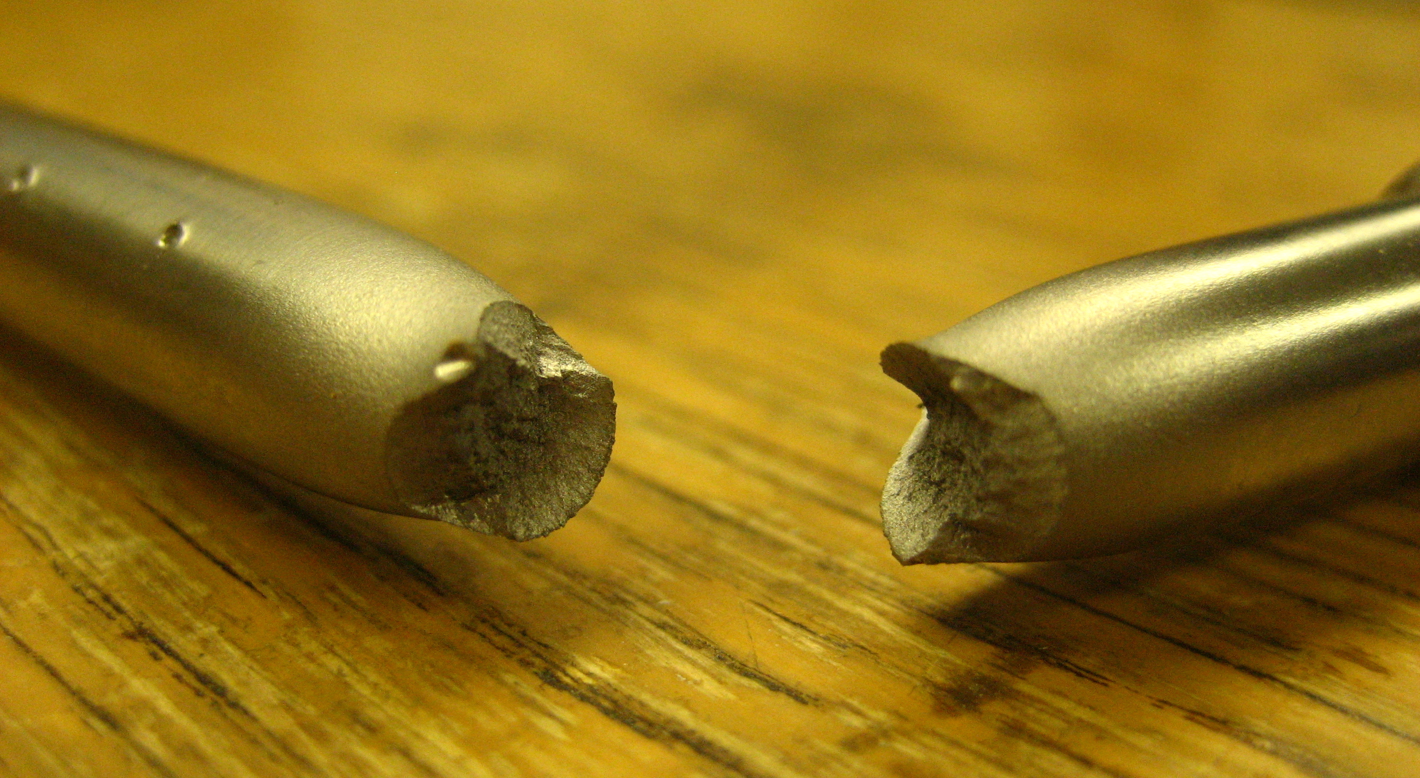
Fracture is the separation of an object or material into two or more pieces under the action of stress. The fracture of a solid usually occurs due to the development of certain displacement discontinuity surfaces within the solid. If a displacement develops perpendicular to the surface, it is called a normal tensile crack or simply a crack; if a displacement develops tangentially, it is called a shear crack, slip band or dislocation. Brittle fractures occur with no apparent deformation before fracture. Ductile fractures occur after visible deformation. Fracture strength, or breaking strength, is the stress when a specimen fails or fractures. The detailed understanding of how a fracture occurs and develops in materials is the object of fracture mechanics. Strength Fracture strength, also known as breaking strength, is the stress at which a specimen fails via fracture. This is usually determined for a given specimen by a tensile test, which charts the stress–strain cu ... [...More Info...] [...Related Items...] OR: [Wikipedia] [Google] [Baidu] |


