|
Nanotextured Surface
A nanotextured surface (NTS) is a surface which is covered with nano-sized structures. Such surfaces have one dimension on the nanoscale, i.e., only the thickness of the surface of an object is between 0.1 and 100 nm. They are currently gaining popularity because of their special applications due to their unique physical properties. Nanotextured surfaces are in various forms like cones, columns, or fibers. These are water, ice, oil, and microorganism repellent that is superamphiphobic, anti-icing, and antifouling respectively and thus self-cleaning. They are simultaneously anti-reflective and transparent, hence they are termed ''smart'' surfaces. In research published online October 21, 2013, in Advanced Materials, of a group of scientists at the U.S. Department of Energy's Brookhaven National Laboratory (BNL), led by BNL physicist and lead author Antonio Checco, proposed that nanotexturing surfaces in the form of cones produces highly water-repellent surfaces. These nano-co ... [...More Info...] [...Related Items...] OR: [Wikipedia] [Google] [Baidu] |
Nanotechnology
Nanotechnology, also shortened to nanotech, is the use of matter on an atomic, molecular, and supramolecular scale for industrial purposes. The earliest, widespread description of nanotechnology referred to the particular technological goal of precisely manipulating atoms and molecules for fabrication of macroscale products, also now referred to as molecular nanotechnology. A more generalized description of nanotechnology was subsequently established by the National Nanotechnology Initiative, which defined nanotechnology as the manipulation of matter with at least one dimension sized from 1 to 100 nanometers (nm). This definition reflects the fact that quantum mechanical effects are important at this quantum-realm scale, and so the definition shifted from a particular technological goal to a research category inclusive of all types of research and technologies that deal with the special properties of matter which occur below the given size threshold. It is therefore commo ... [...More Info...] [...Related Items...] OR: [Wikipedia] [Google] [Baidu] |
Nanofoam
Nanofoams are a class of nanostructured, porous materials (foams) containing a significant population of pores with diameters less than 100 nm. Aerogels are one example of nanofoam. Metal Overview Metallic nanofoams are a subcategorization of nanofoams; more specifically, there are nanofoams consisting of metals, often pure, that form interconnected networks of ligaments that make up the structure of the foam. A variety of metals are used, including copper, nickel, gold, and platinum. Metallic nanofoams may offer certain advantages over alternative polymer nanofoams; structurally, they retain the electrical conductivity of metals, offer increased ductility, as well as the higher surface area and nano-architecture properties offered by nanofoams. Fabrication Synthesis of metallic nanofoams may be accomplished through a variety of methods. In 2006, researchers produced metal nanofoams by igniting pellets of energetic metal bis(tetrazolato)amine complexes. Nanofoams of iro ... [...More Info...] [...Related Items...] OR: [Wikipedia] [Google] [Baidu] |
Display Technology
A display device is an output device for presentation of information in visual or tactile form (the latter used for example in tactile electronic displays for blind people). When the input information that is supplied has an electrical signal the display is called an ''electronic display''. Common applications for ''electronic visual displays'' are television sets or computer monitors. Types of electronic displays In use These are the technologies used to create the various displays in use today. * Liquid crystal display (LCD) ** Light-emitting diode (LED) backlit LCD ** Thin-film transistor (TFT) LCD ** Quantum dot (QLED) display * Light-emitting diode (LED) display ** OLED display ** AMOLED display ** Super AMOLED display Segment displays Some displays can show only digits or alphanumeric characters. They are called segment displays, because they are composed of several segments that switch on and off to give appearance of desired glyph. The segments are usu ... [...More Info...] [...Related Items...] OR: [Wikipedia] [Google] [Baidu] |
Nanomaterials
* Nanomaterials describe, in principle, materials of which a single unit is sized (in at least one dimension) between 1 and 100 nm (the usual definition of nanoscale). Nanomaterials research takes a materials science-based approach to nanotechnology, leveraging advances in materials metrology and synthesis which have been developed in support of microfabrication research. Materials with structure at the nanoscale often have unique optical, electronic, thermo-physical or mechanical properties. Nanomaterials are slowly becoming commercialized and beginning to emerge as commodities. Definition In ISO/TS 80004, ''nanomaterial'' is defined as the "material with any external dimension in the nanoscale or having internal structure or surface structure in the nanoscale", with ''nanoscale'' defined as the "length range approximately from 1 nm to 100 nm". This includes both ''nano-objects'', which are discrete pieces of material, and ''nanostructured materials'', which have i ... [...More Info...] [...Related Items...] OR: [Wikipedia] [Google] [Baidu] |
Sculptured Thin Film
Sculptured thin films (STFs) are nanostructured materials with unidirectionally varying properties that can be designed and realized in a controllable manner using variants of physical vapor deposition. The ability to virtually instantaneously change the growth direction of their columnar morphology, through simple variations in the direction of the incident vapor flux, leads to a wide spectrum of columnar forms. Forms These forms can be: # two-dimensional, ranging from the simple slanted columns and chevrons to the more complex C- and S-shaped morphologies # three-dimensional, including simple helixes and superhelixes # combinations of two- and three-dimensional forms. Properties The column diameter and the column separation normal to the thickness direction of any STF are nominally constant. The column diameter can range from about 10 to 300 nm, while the density may lie between its theoretical maximum value to less than 20% thereof. The crystallinity must be at a scale sm ... [...More Info...] [...Related Items...] OR: [Wikipedia] [Google] [Baidu] |
Quantum Heterostructure
A quantum heterostructure is a heterostructure in a substrate (usually a semiconductor material), where size restricts the movements of the charge carriers forcing them into a quantum confinement. This leads to the formation of a set of discrete energy levels at which the carriers can exist. Quantum heterostructures have sharper density of states than structures of more conventional sizes. Quantum heterostructures are important for fabrication of short-wavelength light-emitting diodes and diode lasers, and for other optoelectronic applications, e.g. high-efficiency photovoltaic cells. Examples of quantum heterostructures confining the carriers in quasi-two, -one and -zero dimensions are: * Quantum wells * Quantum wire In mesoscopic physics, a quantum wire is an electrically conducting wire in which quantum effects influence the transport properties. Usually such effects appear in the dimension of nanometers, so they are also referred to as nanowires. Quantum e ...s * Quantum d ... [...More Info...] [...Related Items...] OR: [Wikipedia] [Google] [Baidu] |
Quantum Dot
Quantum dots (QDs) are semiconductor particles a few nanometres in size, having optical and electronic properties that differ from those of larger particles as a result of quantum mechanics. They are a central topic in nanotechnology. When the quantum dots are illuminated by UV light, an electron in the quantum dot can be excited to a state of higher energy. In the case of a semiconducting quantum dot, this process corresponds to the transition of an electron from the valence band to the conductance band. The excited electron can drop back into the valence band releasing its energy as light. This light emission (photoluminescence) is illustrated in the figure on the right. The color of that light depends on the energy difference between the conductance band and the valence band, or the transition between discrete energy states when band structure is no longer a good definition in QDs. In the language of materials science, nanoscale semiconductor materials tightly confine ... [...More Info...] [...Related Items...] OR: [Wikipedia] [Google] [Baidu] |
Nanoshell
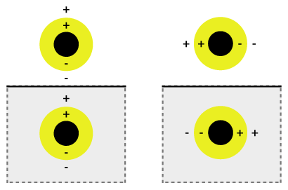
A nanoshell, or rather a nanoshell plasmon, is a type of spherical nanoparticle consisting of a dielectric core which is covered by a thin metallic shell (usually gold). These nanoshells involve a quasiparticle called a plasmon which is a collective excitation or quantum plasma oscillation where the electrons simultaneously oscillate with respect to all the ions. The simultaneous oscillation can be called plasmon hybridization where the tunability of the oscillation is associated with mixture of the inner and outer shell where they hybridize to give a lower energy or higher energy. This lower energy couples strongly to incident light, whereas the higher energy is an anti-bonding and weakly combines to incident light. The hybridization interaction is stronger for thinner shell layers, hence, the thickness of the shell and overall particle radius determines which wavelength of light it couples with. Nanoshells can be varied across a broad range of the light spectrum that spans t ... [...More Info...] [...Related Items...] OR: [Wikipedia] [Google] [Baidu] |
Nanorod
In nanotechnology, nanorods are one morphology of nanoscale objects. Each of their dimensions range from 1–100 nm. They may be synthesized from metals or semiconducting materials. Standard aspect ratios (length divided by width) are 3-5. Nanorods are produced by direct chemical synthesis. A combination of ligands act as shape control agents and bond to different facets of the nanorod with different strengths. This allows different faces of the nanorod to grow at different rates, producing an elongated object. One potential application of nanorods is in display technologies, because the reflectivity of the rods can be changed by changing their orientation with an applied electric field. Another application is for microelectromechanical systems (MEMS). Nanorods, along with other noble metal nanoparticles, also function as theragnostic agents. Nanorods absorb in the near IR, and generate heat when excited with IR light. This property has led to the use of nanorods as cance ... [...More Info...] [...Related Items...] OR: [Wikipedia] [Google] [Baidu] |
Nanoring
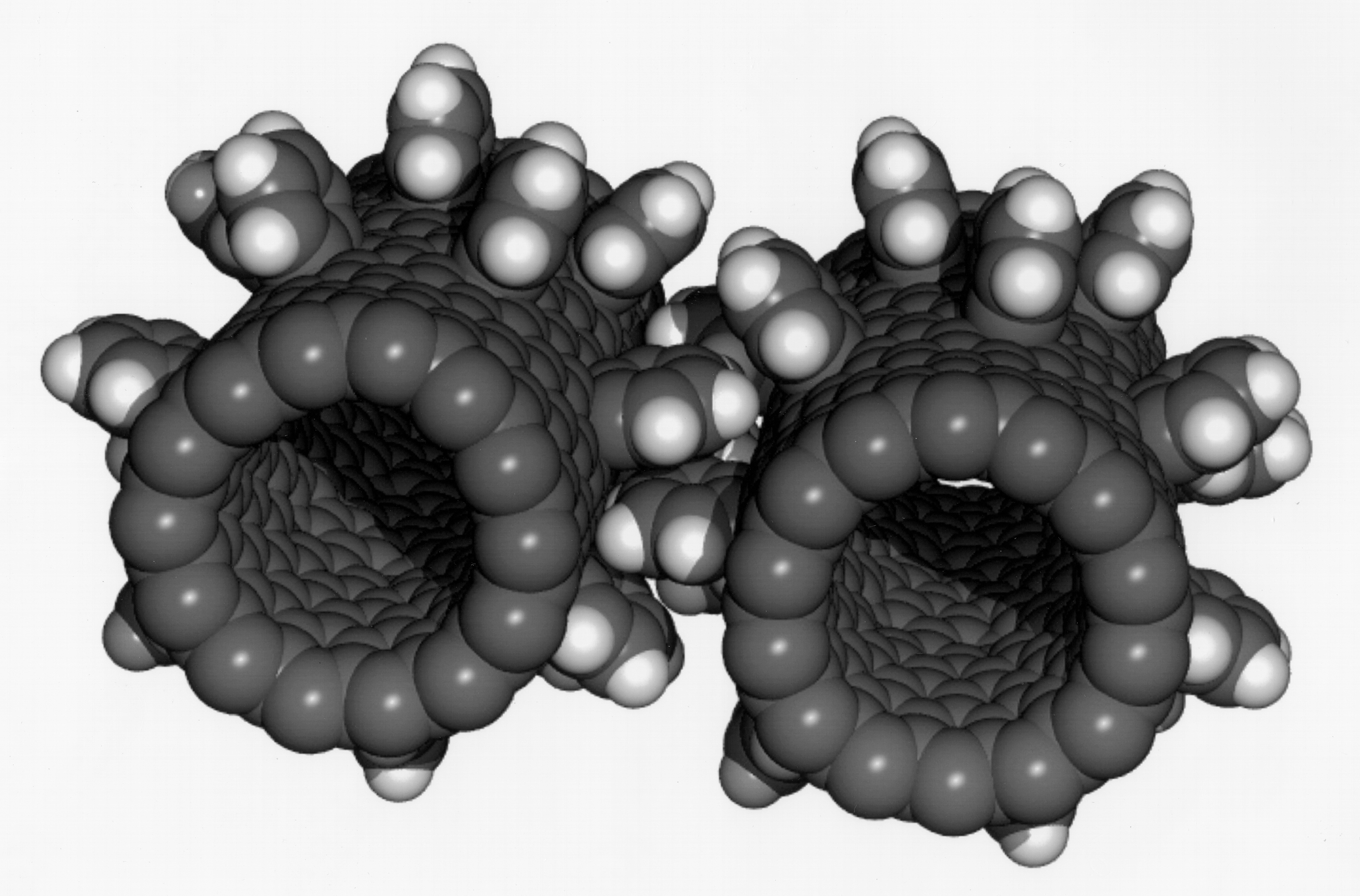
A nanoring is a cyclic nanostructure with a thickness small enough to be on the Nanoscopic scale, nanoscale (10−9 meters). Note that this definition allows the diameter of the ring to be larger than the nanoscale. Nanorings are a relatively recent development within the realm of nanoscience; the first peer-reviewed journal article mentioning these nanostructures came from researchers at the Institute of Physics and Center for Condensed Matter Physics in Beijing who synthesized nanorings made of gallium nitride in 2001. Zinc oxide, a compound very commonly used in nanostructures, was first synthesized into nanorings by researchers at Georgia Institute of Technology in 2004 and several other common nanostructure compounds have been synthesized into nanorings since. More recently, carbon-based nanorings have been synthesized from cyclo-para-phenylenes as well as porphyrins. Overview Although nanorings may have a diameter on the nanoscale, many of these materials have diameters which ... [...More Info...] [...Related Items...] OR: [Wikipedia] [Google] [Baidu] |
Nanopin Film
Nanopin film is an experimental material in nanotechnology developed in 2005 with unusual superhydrophobic properties . A droplet of water makes contact with the surface of this film and forms an almost perfect sphere with a contact angle of 178 °. This happens because it is covered with nanoscale, topped-off pins or cones perpendicular to the surface. The surface is regarded as a composite material with mostly air and a small fraction constituted by the tops of the cones. When the contact angle of the cone material is sufficiently large, Cassie's law predicts large contact angle values for the composite. This particular nanopin film is produced with borosilicate glass. A solution of CoCl2•6H2O or cobalt chloride hexahydrate is heated at 60 °C for 24 hours in a chemical bath deposition to form a brucite type cobalt(II) hydroxide layer with composition :CoOH1.13Cl0.09(CO3)0.39.0.05H20 The top coating is provided by lauric acid in a separate step. A 3 square micrometer surfac ... [...More Info...] [...Related Items...] OR: [Wikipedia] [Google] [Baidu] |
Nanopillar
Nanopillars is an emerging technology within the field of nanostructures. Nanopillars are pillar shaped nanostructures approximately 10 nanometers in diameter that can be grouped together in lattice like arrays. They are a type of metamaterial, which means that nanopillars get their attributes from being grouped into artificially designed structures and not their natural properties. Nanopillars set themselves apart from other nanostructures due to their unique shape. Each nanopillar has a pillar shape at the bottom and a tapered pointy end on top. This shape in combination with nanopillars' ability to be grouped together exhibits many useful properties. Nanopillars have many applications including efficient solar panels, high resolution analysis, and antibacterial surfaces. Applications Solar panels Due to their tapered ends, nanopillars are very efficient at capturing light. Solar collector surfaces coated with nanopillars are three times as efficient as nanowire solar cells. L ... [...More Info...] [...Related Items...] OR: [Wikipedia] [Google] [Baidu] |


