|
Design Closure
Design Closure is a part of the digital electronic design automation workflow by which an integrated circuit (i.e. VLSI) design is modified from its initial description to meet a growing list of design constraints and objectives. Every step in the IC design (such as static timing analysis, placement, routing, and so on) is already complex and often forms its own field of study. This article, however, looks at the overall design closure process, which takes a chip from its initial design state to the final form in which all of its design constraints are met. Introduction Every chip starts off as someone’s idea of a good thing: "If we can make a part that performs function X, we will all be rich!" Once the concept is established, someone from marketing says "To make this chip profitably, it must cost $C and run at frequency F." Someone from manufacturing says "To meet this chip’s targets, it must have a yield of Y%." Someone from packaging says “It must fit in the P pac ... [...More Info...] [...Related Items...] OR: [Wikipedia] [Google] [Baidu] |
Design Flow (EDA)
Design flows are the explicit combination of electronic design automation tools to accomplish the design of an integrated circuit. Moore's law has driven the entire IC implementation RTL to GDSII design flows from one which uses primarily stand-alone synthesis, placement, and routing algorithms to an integrated construction and analysis flows for design closure. The challenges of rising interconnect delay led to a new way of thinking about and integrating design closure tools. The RTL to GDSII flow underwent significant changes from 1980 through 2005. The continued scaling of CMOS technologies significantly changed the objectives of the various design steps. The lack of good predictors for delay has led to significant changes in recent design flows. New scaling challenges such as leakage power, variability, and reliability will continue to require significant changes to the design closure process in the future. Many factors describe what drove the design flow from a set of s ... [...More Info...] [...Related Items...] OR: [Wikipedia] [Google] [Baidu] |
Signoff (EDA)
In the automated design of integrated circuits, signoff (also written as sign-off) checks is the collective name given to a series of verification steps that the design must pass before it can be taped out. This implies an iterative process involving incremental fixes across the board using one or more check types, and then retesting the design. There are two types of sign-off's: front-end sign-off and back-end sign-off. After back-end sign-off the chip goes to fabrication. After listing out all the features in the specification, the verification engineer will write coverage for those features to identify bugs, and send back the RTL design to the designer. Bugs, or defects, can include issues like missing features (comparing the layout to the specification), errors in design (typo and functional errors), etc. When the coverage reaches a maximum% then the verification team will sign it off. By using a methodology like UVM, OVM, or VMM, the verification team develops a reusable envi ... [...More Info...] [...Related Items...] OR: [Wikipedia] [Google] [Baidu] |
Electronic Design
''Electronic Design'' magazine, founded in 1952, is an electronics and electrical engineering trade magazine and website. History Hayden Publishing Company began publishing the bi-weekly magazine Electronic Design in December 1952, and was later published by InformaUSA, Inc. In 1986, Verenigde Nederlandse Uitgeverijen, purchased Hayden Publishing Inc. In June 1988, Verenigde Nederlandse Uitgeverijen, purchased ''Electronic Design'' from McGraw-Hill. In July 1989, Penton Media, purchased ''Electronic Design'', then in Hasbrouck, N.J., from Verenigde Nederlandse Uitgeverijen. In July 2007, Penton Media's OEM electronics publication, ''EE Product News'', merged with Penton Media's "Electronic Design" magazine. ''EE Product News'' was founded in 1941, as a monthly publication. In September 2016, Informa, purchased Penton Media, including ''Electronic Design''. In November 2019, Endeavor Business Media purchased ''Electronic Design'' from Informa. Content Sections i ... [...More Info...] [...Related Items...] OR: [Wikipedia] [Google] [Baidu] |
Electronic Design Automation
Electronic design automation (EDA), also referred to as electronic computer-aided design (ECAD), is a category of software tools for designing Electronics, electronic systems such as integrated circuits and printed circuit boards. The tools work together in a Design flow (EDA), design flow that chip designers use to design and analyze entire semiconductor chips. Since a modern semiconductor chip can have billions of components, EDA tools are essential for their design; this article in particular describes EDA specifically with respect to integrated circuits (ICs). History Early days Prior to the development of EDA, integrated circuits were designed by hand and manually laid out. Some advanced shops used geometric software to generate tapes for a Gerber format, Gerber photoplotter, responsible for generating a monochromatic exposure image, but even those copied digital recordings of mechanically drawn components. The process was fundamentally graphic, with the translation f ... [...More Info...] [...Related Items...] OR: [Wikipedia] [Google] [Baidu] |
Integrated Circuit Design
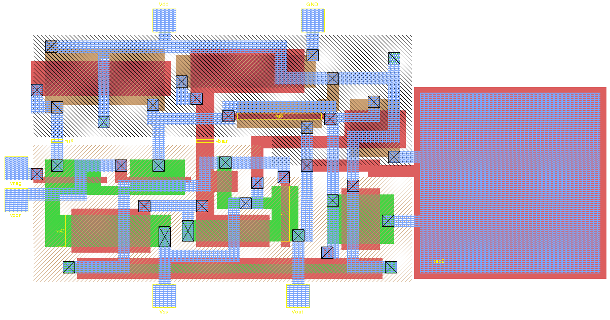
Integrated circuit design, or IC design, is a sub-field of electronics engineering, encompassing the particular logic and circuit design techniques required to design integrated circuits, or ICs. ICs consist of miniaturized electronic components built into an electrical network on a monolithic semiconductor substrate by photolithography. IC design can be divided into the broad categories of digital and analog IC design. Digital IC design is to produce components such as microprocessors, FPGAs, memories (RAM, ROM, and flash) and digital ASICs. Digital design focuses on logical correctness, maximizing circuit density, and placing circuits so that clock and timing signals are routed efficiently. Analog IC design also has specializations in power IC design and RF IC design. Analog IC design is used in the design of op-amps, linear regulators, phase locked loops, oscillators and active filters. Analog design is more concerned with the physics of the semiconductor devices such as ... [...More Info...] [...Related Items...] OR: [Wikipedia] [Google] [Baidu] |
Electronic Design Automation
Electronic design automation (EDA), also referred to as electronic computer-aided design (ECAD), is a category of software tools for designing Electronics, electronic systems such as integrated circuits and printed circuit boards. The tools work together in a Design flow (EDA), design flow that chip designers use to design and analyze entire semiconductor chips. Since a modern semiconductor chip can have billions of components, EDA tools are essential for their design; this article in particular describes EDA specifically with respect to integrated circuits (ICs). History Early days Prior to the development of EDA, integrated circuits were designed by hand and manually laid out. Some advanced shops used geometric software to generate tapes for a Gerber format, Gerber photoplotter, responsible for generating a monochromatic exposure image, but even those copied digital recordings of mechanically drawn components. The process was fundamentally graphic, with the translation f ... [...More Info...] [...Related Items...] OR: [Wikipedia] [Google] [Baidu] |
International Technology Roadmap For Semiconductors
The International Technology Roadmap for Semiconductors (ITRS) is a set of documents produced by a group of semiconductor industry experts. These experts are representative of the sponsoring organisations which include the Semiconductor Industry Associations of Taiwan, South Korea, the United States, Europe, Japan, and China. As of 2017, ITRS is no longer being updated. Its successor is the International Roadmap for Devices and Systems. The documents carried disclaimer: "The ITRS is devised and intended for technology assessment only and is without regard to any commercial considerations pertaining to individual products or equipment". The documents represent best opinion on the directions of research and time-lines up to about 15 years into the future for the following areas of technology: History Constructing an integrated circuit, or any semiconductor device, requires a series of operations—photolithography, etching, metal deposition, and so on. As the industry evolved, ... [...More Info...] [...Related Items...] OR: [Wikipedia] [Google] [Baidu] |
Mask Data Preparation
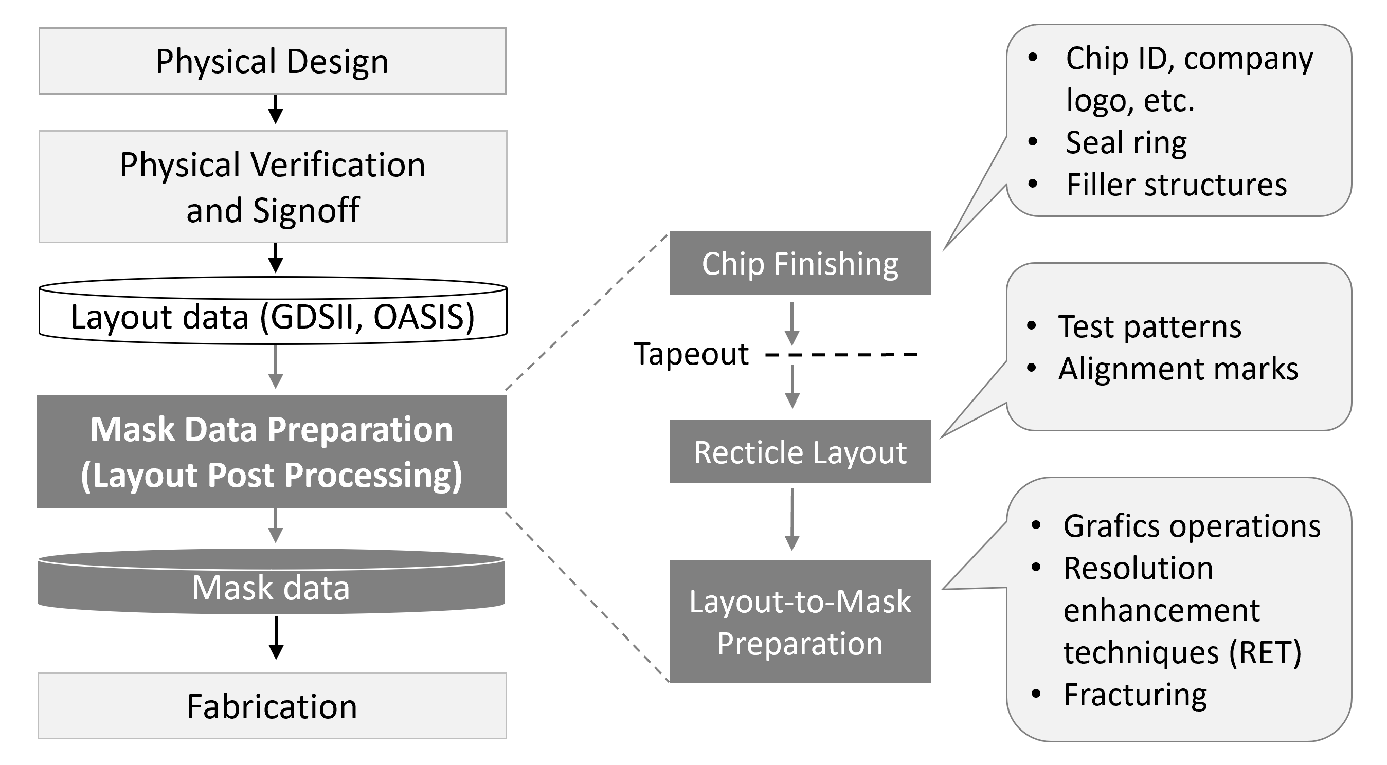
Mask data preparation (MDP), also known as layout post processing, is the procedure of translating a file containing the intended set of polygons from an integrated circuit layout into set of instructions that a photomask writer can use to generate a physical mask. Typically, amendments and additions to the chip layout are performed in order to convert the physical layout into data for mask production. Mask data preparation requires an input file which is in a GDSII or OASIS format, and produces a file that is in a proprietary format specific to the mask writer. MDP procedures Although historically converting the physical layout into data for mask production was relatively simple, more recent MDP procedures require various procedures: * ''Chip finishing'' which includes custom designations and structures to improve manufacturability of the layout. Examples of the latter are a seal ring and filler structures. * Producing a ''reticle layout'' with test patterns and alignment ... [...More Info...] [...Related Items...] OR: [Wikipedia] [Google] [Baidu] |
Photomask
A photomask is an opaque plate with holes or transparencies that allow light to shine through in a defined pattern. They are commonly used in photolithography and the production of integrated circuits (ICs or "chips") in particular. Masks are used to produce a pattern on a substrate, normally a thin slice of silicon known as a wafer in the case of chip manufacturing. Several masks are used in turn, each one reproducing a layer of the completed design, and together they are known as a mask set. Previously, photomasks used to be produced manually by using rubylith and mylar. As complexity continued to grow, manual processing of any sort became difficult. This was solved with the introduction of the optical pattern generator which automated the process of producing the initial large-scale pattern, and the step-and-repeat cameras that automated the copying of the pattern into a multiple-IC mask. The intermediate masks are known as reticles, and were initially copied to production mas ... [...More Info...] [...Related Items...] OR: [Wikipedia] [Google] [Baidu] |
Tape-out
In electronics and photonics design, tape-out or tapeout is the final result of the design process for integrated circuits or printed circuit boards before they are sent for manufacturing. The tapeout is specifically the point at which the graphic for the photomask of the circuit is sent to the fabrication facility. History Historically, the term references the early days of printed circuit design, when the enlarged (for higher precision) "artwork" for the photomask was manually "taped out" using black line tape (commonly Bishop Graphics crepe) and also Rubylith sheets. In the post-war era of the 1940–50s, the techniques developed for rapid and low-cost circuit reproduction evolved to photographically replicated 2D manufacturing. The verb "to tapeout" was already widely used for the process and adopted for transistor fabrication, which evolved to full integrated-circuit approaches. Procedures involved The term ''tapeout'' currently is used to describe the creation of the p ... [...More Info...] [...Related Items...] OR: [Wikipedia] [Google] [Baidu] |
Design Rule Checking
In electronic design automation, a design rule is a geometric constraint imposed on circuit board, semiconductor device, and integrated circuit (IC) designers to ensure their designs function properly, reliably, and can be produced with acceptable yield. Design rules for production are developed by process engineers based on the capability of their processes to realize design intent. Electronic design automation is used extensively to ensure that designers do not violate design rules; a process called design rule checking (DRC). DRC is a major step during physical verification signoff on the design, which also involves LVS (layout versus schematic) checks, XOR checks, ERC ( electrical rule check), and antenna checks. The importance of design rules and DRC is greatest for ICs, which have micro- or nano-scale geometries; for advanced processes, some fabs also insist upon the use of more restricted rules to improve yield. Design rules Design rules are a series of parameters provi ... [...More Info...] [...Related Items...] OR: [Wikipedia] [Google] [Baidu] |

