|
RHPPC
The RHPPC is a radiation hardened processor based on PowerPC 603e technology licensed from Motorola (now Freescale) and manufactured by Honeywell. The RHPPC is equivalent to the commercial PowerPC 603e processor with the minor exceptions of the phase locked loop (PLL) and the processor version register (PVR). The RHPPC processor is compatible with the PowerPC architecture (Book I-III), the PowerPC 603e programmers interface and is also supported by common PowerPC software tools and embedded operating systems, like VxWorks. Technical details The RHPPC processor generates 190 MIPS with the Dhrystone mix with its core clock at 100 MHz (i.e. the RHPPC processor completes 1.9 instructions per cycle). The RHPPC runs with a 25, 33.3, 40, or 50 MHz 60x bus clock (SYSCLK) which is generated based on the PCI clock. The 60x bus clock is de-skewed on-chip by a PLL and can also be multiplied. The RHPPC processor is a superscalar machine with five execution units: system regis ... [...More Info...] [...Related Items...] OR: [Wikipedia] [Google] [Baidu] |
Radiation Hardened
Radiation hardening is the process of making electronic components and circuits resistant to damage or malfunction caused by high levels of ionizing radiation (particle radiation and high-energy electromagnetic radiation), especially for environments in outer space (especially beyond low Earth orbit), around nuclear reactors and particle accelerators, or during nuclear accidents or nuclear warfare. Most semiconductor electronic components are susceptible to radiation damage, and radiation-hardened (rad-hard) components are based on their non-hardened equivalents, with some design and manufacturing variations that reduce the susceptibility to radiation damage. Due to the low demand and the extensive development and testing required to produce a radiation-tolerant design of a microelectronic chip, the technology of radiation-hardened chips tends to lag behind the most recent developments. They also typically cost more than their commercial counterparts. Radiation-hardened product ... [...More Info...] [...Related Items...] OR: [Wikipedia] [Google] [Baidu] |
PowerPC 603e
The PowerPC 600 family was the first family of PowerPC processors built. They were designed at the Somerset facility in Austin, Texas, jointly funded and staffed by engineers from IBM and Motorola as a part of the AIM alliance. Somerset was opened in 1992 and its goal was to make the first PowerPC processor and then keep designing general purpose PowerPC processors for personal computers. The first incarnation became the PowerPC 601 in 1993, and the second generation soon followed with the PowerPC 603, PowerPC 604 and the 64-bit PowerPC 620. Nuclear family PowerPC 601 The PowerPC 601 was the first generation of microprocessors to support the basic 32-bit PowerPC instruction set. The design effort started in earnest in mid-1991 and the first prototype chips were available in October 1992. The first 601 processors were introduced in an IBM RS/6000 workstation in October 1993 (alongside its more powerful multichip cousin IBM POWER2 line of processors) and the first Apple Power ... [...More Info...] [...Related Items...] OR: [Wikipedia] [Google] [Baidu] |
Floating Point Unit
A floating-point unit (FPU), numeric processing unit (NPU), colloquially math coprocessor, is a part of a computer system specially designed to carry out operations on floating-point numbers. Typical operations are addition, subtraction, multiplication, division, and square root. Modern designs generally include a fused multiply-add instruction, which was found to be very common in real-world code. Some FPUs can also perform various transcendental functions such as exponential or trigonometric calculations, but the accuracy can be low, so some systems prefer to compute these functions in software. Floating-point operations were originally handled in software in early computers. Over time, manufacturers began to provide standardized floating-point libraries as part of their software collections. Some machines, those dedicated to scientific processing, would include specialized hardware to perform some of these tasks with much greater speed. The introduction of microcode in the ... [...More Info...] [...Related Items...] OR: [Wikipedia] [Google] [Baidu] |
PowerPC Microprocessors
PowerPC (with the backronym Performance Optimization With Enhanced RISC – Performance Computing, sometimes abbreviated as PPC) is a reduced instruction set computer (RISC) instruction set architecture (ISA) created by the 1991 Apple–IBM–Motorola alliance, known as AIM. PowerPC, as an evolving instruction set, has been named Power ISA since 2006, while the old name lives on as a trademark for some implementations of Power Architecture–based processors. Originally intended for personal computers, the architecture is well known for being used by Apple's desktop and laptop lines from 1994 until 2006, and in several videogame consoles including Microsoft's Xbox 360, Sony's PlayStation 3, and Nintendo's GameCube, Wii, and Wii U. PowerPC was also used for the Curiosity and Perseverance rovers on Mars and a variety of satellites. It has since become a niche architecture for personal computers, particularly with AmigaOS 4 implementations, but remains popular for embedded syste ... [...More Info...] [...Related Items...] OR: [Wikipedia] [Google] [Baidu] |
Wire Bonding
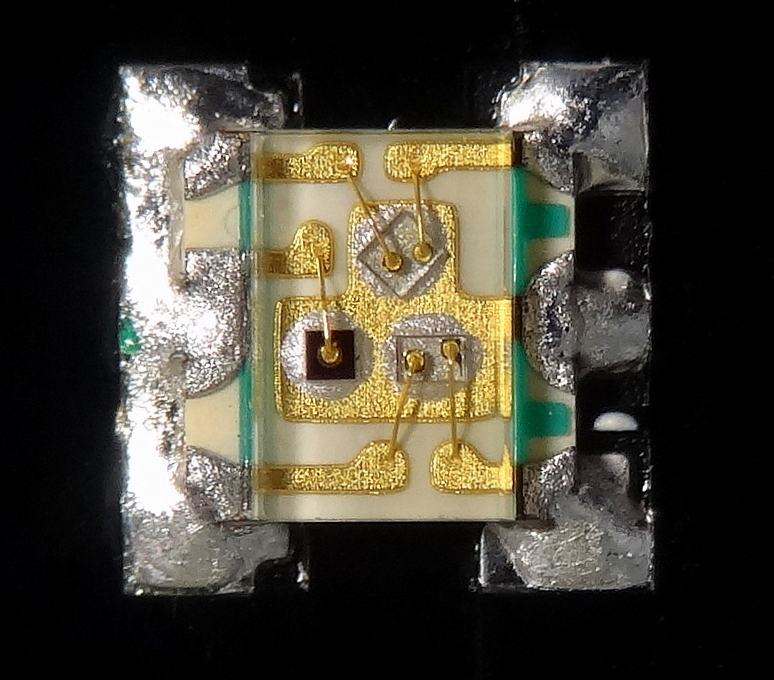
Wire bonding is a method of making interconnections between an integrated circuit (IC) or other semiconductor device and its packaging during semiconductor device fabrication. Wire bonding can also be used to connect an IC to other electronics or to connect from one printed circuit board (PCB) to another, although these are less common. Wire bonding is generally considered the most cost-effective and flexible interconnect technology and is used to assemble the vast majority of semiconductor packages. Wire bonding can be used at frequencies above 100 GHz. [...More Info...] [...Related Items...] OR: [Wikipedia] [Google] [Baidu] |
Ball Grid Array
A ball grid array (BGA) is a type of surface-mount packaging (a chip carrier) used for integrated circuits. BGA packages are used to permanently mount devices such as microprocessors. A BGA can provide more interconnection pins than can be put on a dual in-line or flat package. The whole bottom surface of the device can be used, instead of just the perimeter. The traces connecting the package's leads to the wires or balls which connect the die to package are also on average shorter than with a perimeter-only type, leading to better performance at high speeds. Soldering of BGA devices requires precise control and is usually done by automated processes such as in computer-controlled automatic reflow ovens. Description The BGA is descended from the pin grid array (PGA), which is a package with one face covered (or partly covered) with pins in a grid pattern which, in operation, conduct electrical signals between the integrated circuit and the printed circuit board (PCB) ... [...More Info...] [...Related Items...] OR: [Wikipedia] [Google] [Baidu] |
Surface-mount Technology
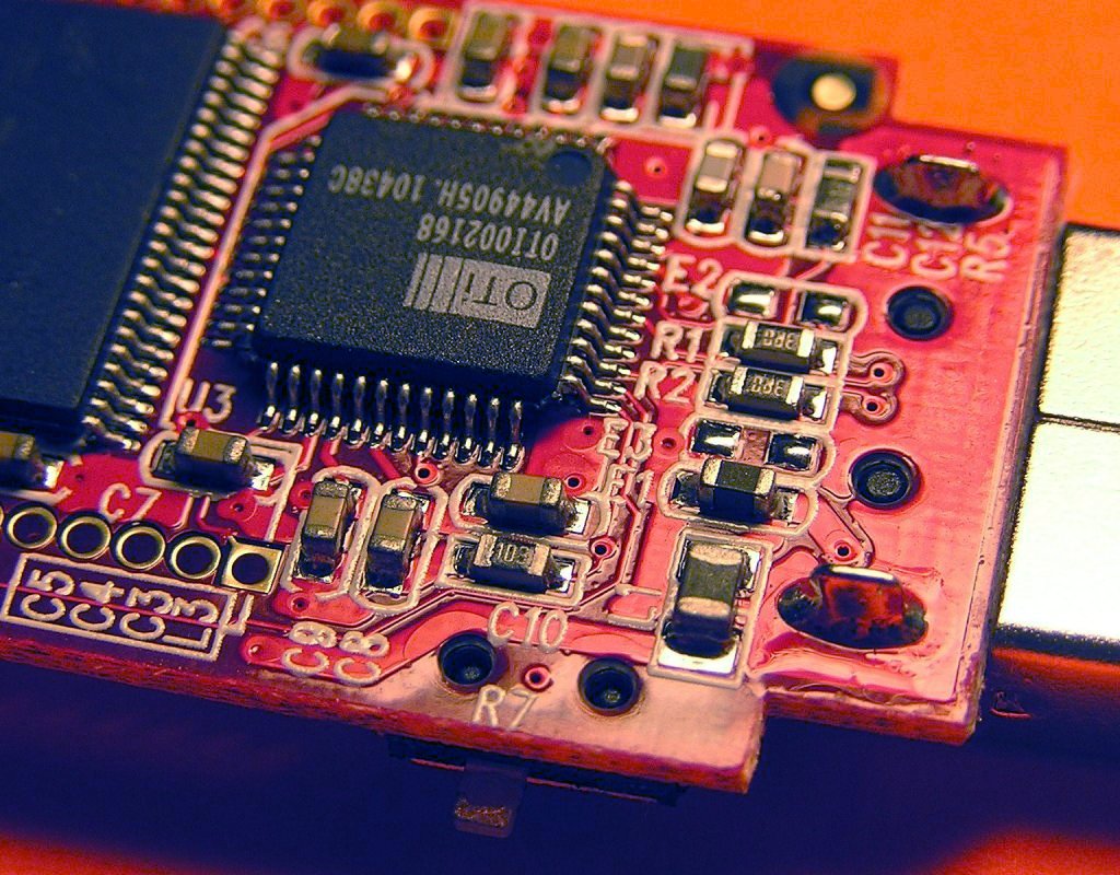
Surface-mount technology (SMT), originally called planar mounting, is a method in which the electrical components are mounted directly onto the surface of a printed circuit board (PCB). An electrical component mounted in this manner is referred to as a surface-mount device (SMD). In industry, this approach has largely replaced through-hole technology construction method of fitting components, in large part because SMT allows for increased manufacturing automation which reduces cost and improves quality. It also allows for more components to fit on a given area of substrate. Both technologies can be used on the same board, with the through-hole technology often used for components not suitable for surface mounting such as large transformers and heat-sinked power semiconductors. An SMT component is usually smaller than its through-hole counterpart because it has either smaller leads or no leads at all. It may have short pins or leads of various styles, flat contacts, a matrix of ... [...More Info...] [...Related Items...] OR: [Wikipedia] [Google] [Baidu] |
Aluminium Oxide
Aluminium oxide (or aluminium(III) oxide) is a chemical compound of aluminium and oxygen with the chemical formula . It is the most commonly occurring of several Aluminium oxide (compounds), aluminium oxides, and specifically identified as aluminium oxide. It is commonly called alumina and may also be called aloxide, aloxite, ALOX or alundum in various forms and applications and alumina is refined from bauxite. It occurs naturally in its crystalline Polymorphism (materials science), polymorphic phase (matter), phase α-Al2O3 as the mineral corundum, varieties of which form the precious gemstones ruby and sapphire,which have an alumina content approaching 100%. Al2O3 is used as feedstock to produce aluminium metal, as an abrasive owing to its hardness, and as a refractory material owing to its high melting point. Natural occurrence Corundum is the most common naturally occurring crystallinity, crystalline form of aluminium oxide. ruby, Rubies and sapphires are gem-quality forms o ... [...More Info...] [...Related Items...] OR: [Wikipedia] [Google] [Baidu] |
Silicon On Insulator
In semiconductor manufacturing, silicon on insulator (SOI) technology is fabrication of silicon semiconductor devices in a layered silicon–insulator–silicon substrate, to reduce parasitic capacitance within the device, thereby improving performance. SOI-based devices differ from conventional silicon-built devices in that the silicon junction is above an electrical insulator, typically silicon dioxide or sapphire (these types of devices are called silicon on sapphire, or SOS). The choice of insulator depends largely on intended application, with sapphire being used for high-performance radio frequency (RF) and radiation-sensitive applications, and silicon dioxide for diminished short-channel effects in other microelectronics devices. The insulating layer and topmost silicon layer also vary widely with application. Industry need SOI technology is one of several manufacturing strategies to allow the continued miniaturization of microelectronic devices, colloquially referred to ... [...More Info...] [...Related Items...] OR: [Wikipedia] [Google] [Baidu] |
Semiconductor Fabrication
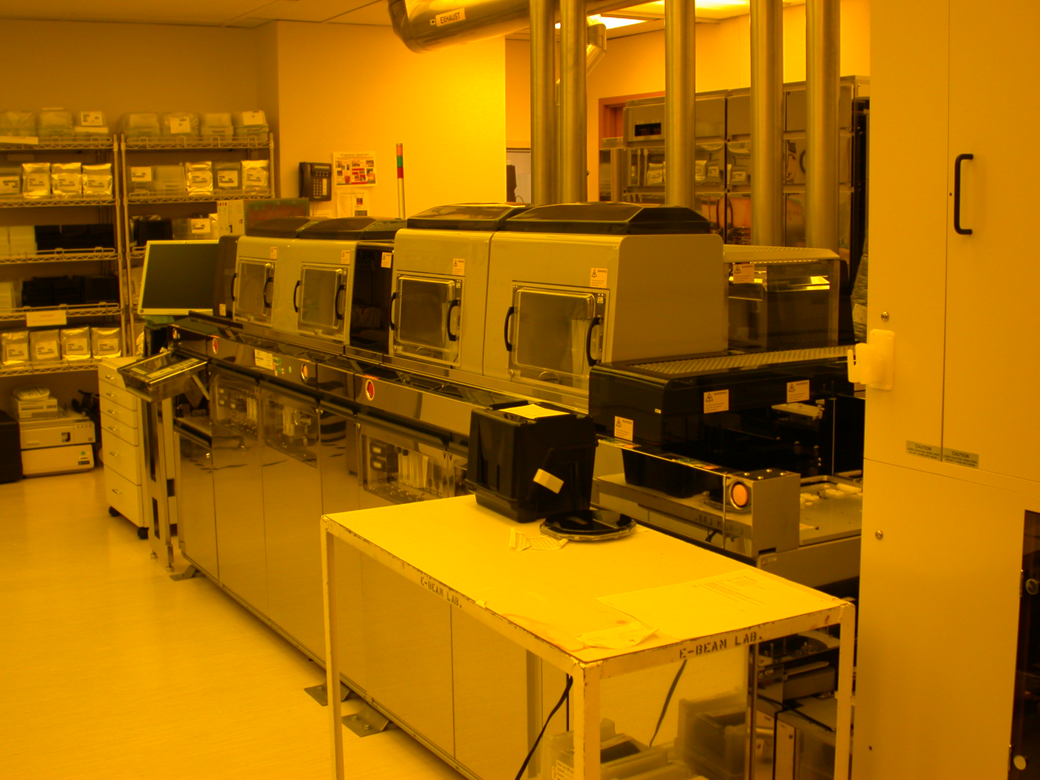
Semiconductor device fabrication is the process used to manufacture semiconductor devices, typically integrated circuits (ICs) such as microprocessors, microcontrollers, and memories (such as RAM and flash memory). It is a multiple-step photolithographic and physico-chemical process (with steps such as thermal oxidation, thin-film deposition, ion-implantation, etching) during which electronic circuits are gradually created on a wafer, typically made of pure single-crystal semiconducting material. Silicon is almost always used, but various compound semiconductors are used for specialized applications. This article focuses on the manufacture of integrated circuits, however steps such as etching and photolithography can be used to manufacture other devices such as LCD and OLED displays. The fabrication process is performed in highly specialized semiconductor fabrication plants, also called foundries or "fabs", with the central part being the " clean room". In more advanced semi ... [...More Info...] [...Related Items...] OR: [Wikipedia] [Google] [Baidu] |
CPU Cache
A CPU cache is a hardware cache used by the central processing unit (CPU) of a computer to reduce the average cost (time or energy) to access data from the main memory. A cache is a smaller, faster memory, located closer to a processor core, which stores copies of the data from frequently used main memory locations. Most CPUs have a hierarchy of multiple cache levels (L1, L2, often L3, and rarely even L4), with different instruction-specific and data-specific caches at level 1. The cache memory is typically implemented with static random-access memory (SRAM), in modern CPUs by far the largest part of them by chip area, but SRAM is not always used for all levels (of I- or D-cache), or even any level, sometimes some latter or all levels are implemented with eDRAM. Other types of caches exist (that are not counted towards the "cache size" of the most important caches mentioned above), such as the translation lookaside buffer (TLB) which is part of the memory management unit (M ... [...More Info...] [...Related Items...] OR: [Wikipedia] [Google] [Baidu] |


