|
Contact Pad
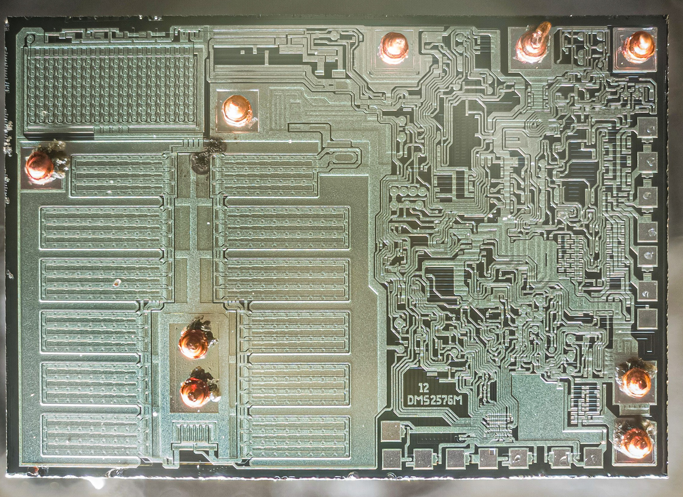
Contact pads or bond pads are small, conductive surface areas of a printed circuit board (PCB) or die of an integrated circuit. They are often made of gold, copper, or aluminum and measure mere micrometres wide. Pads are positioned on the edges of die, to facilitate connections without shorting. Contact pads exist to provide a larger surface area for connections to a microchip or PCB, allowing for the input and output of data and power. Possible methods of connecting contact pads to a system include soldering, wirebonding, or flip chip mounting. Contact pads are created alongside a chip's functional structure during the photolithography steps of the fabrication process, and afterwards they are tested. During the test process, contact pads are probed with the needles of a probe card on Automatic Test Equipment Automatic test equipment or automated test equipment (ATE) is any apparatus that performs tests on a device, known as the device under test (DUT), equipment under t ... [...More Info...] [...Related Items...] OR: [Wikipedia] [Google] [Baidu] |
Printed Circuit Board
A printed circuit board (PCB), also called printed wiring board (PWB), is a Lamination, laminated sandwich structure of electrical conduction, conductive and Insulator (electricity), insulating layers, each with a pattern of traces, planes and other features (similar to wires on a flat surface) Chemical milling, etched from one or more sheet layers of copper laminated onto or between sheet layers of a non-conductive substrate. PCBs are used to connect or Electrical wiring, "wire" Electronic component, components to one another in an electronic circuit. Electrical components may be fixed to conductive pads on the outer layers, generally by soldering, which both electrically connects and mechanically fastens the components to the board. Another manufacturing process adds Via (electronics), vias, metal-lined drilled holes that enable electrical interconnections between conductive layers, to boards with more than a single side. Printed circuit boards are used in nearly all e ... [...More Info...] [...Related Items...] OR: [Wikipedia] [Google] [Baidu] |
Die (integrated Circuit)
A die, in the context of integrated circuits, is a small block of semiconducting material on which a given functional circuit is Semiconductor fabrication, fabricated. Typically, integrated circuits are produced in large batches on a single wafer (electronics), wafer of electronic-grade Monocrystalline silicon, silicon (EGS) or other semiconductor (such as Gallium arsenide, GaAs) through processes such as photolithography. The wafer is cut (wafer dicing, diced) into many pieces, each containing one copy of the circuit. Each of these pieces is called a die. There are three commonly used plural forms: ''dice'', ''dies,'' and ''die''. To simplify handling and integration onto a printed circuit board, most dies are integrated circuit packaging, packaged in List of electronic component packaging types, various forms. Manufacturing process Most dies are composed of silicon and used for integrated circuits. The process begins with the production of Single crystal, monocrystalline sili ... [...More Info...] [...Related Items...] OR: [Wikipedia] [Google] [Baidu] |
Integrated Circuit
An integrated circuit (IC), also known as a microchip or simply chip, is a set of electronic circuits, consisting of various electronic components (such as transistors, resistors, and capacitors) and their interconnections. These components are etched onto a small, flat piece ("chip") of semiconductor material, usually silicon. Integrated circuits are used in a wide range of electronic devices, including computers, smartphones, and televisions, to perform various functions such as processing and storing information. They have greatly impacted the field of electronics by enabling device miniaturization and enhanced functionality. Integrated circuits are orders of magnitude smaller, faster, and less expensive than those constructed of discrete components, allowing a large transistor count. The IC's mass production capability, reliability, and building-block approach to integrated circuit design have ensured the rapid adoption of standardized ICs in place of designs using discre ... [...More Info...] [...Related Items...] OR: [Wikipedia] [Google] [Baidu] |
Micrometre
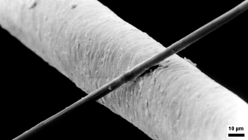
The micrometre (English in the Commonwealth of Nations, Commonwealth English as used by the International Bureau of Weights and Measures; SI symbol: μm) or micrometer (American English), also commonly known by the non-SI term micron, is a unit of length in the International System of Units (SI) equalling (SI standard prefix "micro-" = ); that is, one millionth of a metre (or one thousandth of a millimetre, , or about ). The nearest smaller common SI Unit, SI unit is the nanometre, equivalent to one thousandth of a micrometre, one millionth of a millimetre or one billionth of a metre (). The micrometre is a common unit of measurement for wavelengths of infrared radiation as well as sizes of biological cell (biology), cells and bacteria, and for grading wool by the diameter of the fibres. The width of a single human hair ranges from approximately 20 to . Examples Between 1 μm and 10 μm: * 1–10 μm – length of a typical bacterium * 3–8 μm – width of str ... [...More Info...] [...Related Items...] OR: [Wikipedia] [Google] [Baidu] |
Soldering
Soldering (; ) is a process of joining two metal surfaces together using a filler metal called solder. The soldering process involves heating the surfaces to be joined and melting the solder, which is then allowed to cool and solidify, creating a strong and durable joint. Soldering is commonly used in the electronics industry for the manufacture and repair of Printed circuit board, printed circuit boards (PCBs) and other electronic components. It is also used in plumbing and Metalworking, metalwork, as well as in the manufacture of jewelry and other decorative items. The solder used in the process can vary in composition, with different alloys used for different applications. Common solder alloys include tin-lead, tin-silver, and tin-copper, among others. Lead-free solder has also become more widely used in recent years due to health and environmental concerns associated with the use of lead. In addition to the type of solder used, the temperature and method of heating also p ... [...More Info...] [...Related Items...] OR: [Wikipedia] [Google] [Baidu] |
Wire Bonding
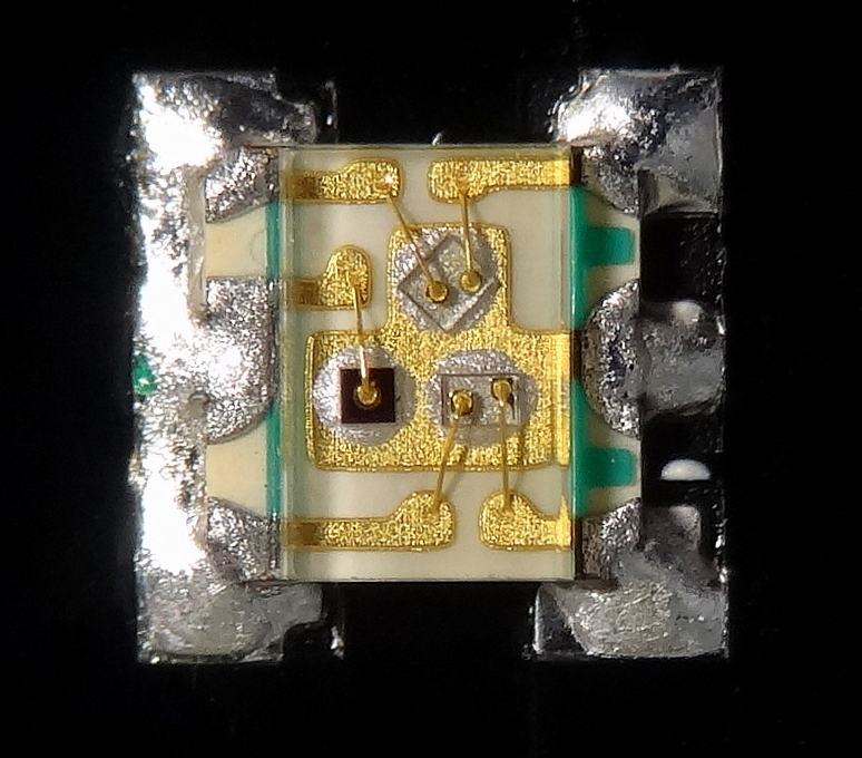
Wire bonding is a method of making interconnections between an integrated circuit (IC) or other semiconductor device and its packaging during semiconductor device fabrication. Wire bonding can also be used to connect an IC to other electronics or to connect from one printed circuit board (PCB) to another, although these are less common. Wire bonding is generally considered the most cost-effective and flexible interconnect technology and is used to assemble the vast majority of semiconductor packages. Wire bonding can be used at frequencies above 100 GHz. [...More Info...] [...Related Items...] OR: [Wikipedia] [Google] [Baidu] |
Flip Chip
Flip chip, also known as controlled collapse chip connection or its abbreviation, C4, is a method for interconnecting dies such as semiconductor devices, IC chips, integrated passive devices and microelectromechanical systems (MEMS), to external circuitry with solder bumps that have been deposited onto the chip pads. The technique was developed by General Electric's Light Military Electronics Department, Utica, New York. The solder bumps are deposited on the chip pads on the top side of the wafer during the final wafer processing step. In order to mount the chip to external circuitry (e.g., a circuit board or another chip or wafer), it is flipped over so that its top side faces down, and aligned so that its pads align with matching pads on the external circuit, and then the solder is reflowed to complete the interconnect. This is in contrast to wire bonding, in which the chip is mounted upright and fine wires are welded onto the chip pads and lead frame contacts to interconne ... [...More Info...] [...Related Items...] OR: [Wikipedia] [Google] [Baidu] |
Photolithography
Photolithography (also known as optical lithography) is a process used in the manufacturing of integrated circuits. It involves using light to transfer a pattern onto a substrate, typically a silicon wafer. The process begins with a photosensitive material, called a photoresist, being applied to the substrate. A photomask that contains the desired pattern is then placed over the photoresist. Light is shone through the photomask, exposing the photoresist in certain areas. The exposed areas undergo a chemical change, making them either soluble or insoluble in a developer solution. After development, the pattern is transferred onto the substrate through etching, chemical vapor deposition, or ion implantation processes. Ultraviolet, Ultraviolet (UV) light is typically used. Photolithography processes can be classified according to the type of light used, including ultraviolet lithography, deep ultraviolet lithography, extreme ultraviolet lithography, extreme ultraviolet lithography ... [...More Info...] [...Related Items...] OR: [Wikipedia] [Google] [Baidu] |
Semiconductor Device Fabrication
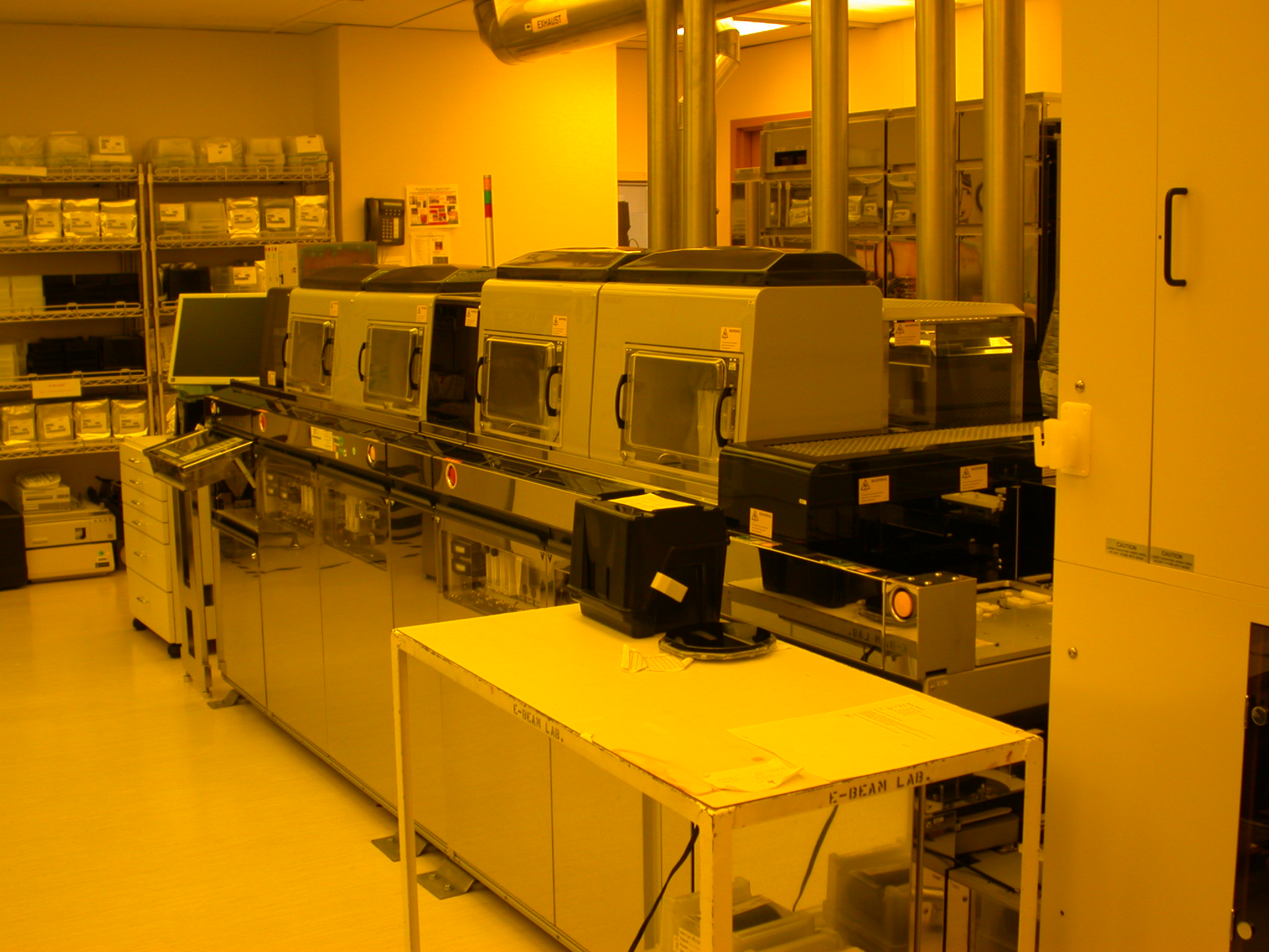
Semiconductor device fabrication is the process used to manufacture semiconductor devices, typically integrated circuits (ICs) such as microprocessors, microcontrollers, and memories (such as Random-access memory, RAM and flash memory). It is a multiple-step Photolithography, photolithographic and physico-chemical process (with steps such as thermal oxidation, thin-film deposition, ion-implantation, etching) during which electronic circuits are gradually created on a wafer (electronics), wafer, typically made of pure single-crystal semiconducting material. Silicon is almost always used, but various compound semiconductors are used for specialized applications. This article focuses on the manufacture of integrated circuits, however steps such as etching and photolithography can be used to manufacture other devices such as LCD and OLED displays. The fabrication process is performed in highly specialized semiconductor fabrication plants, also called foundries or "fabs", with the cen ... [...More Info...] [...Related Items...] OR: [Wikipedia] [Google] [Baidu] |
Wafer Testing
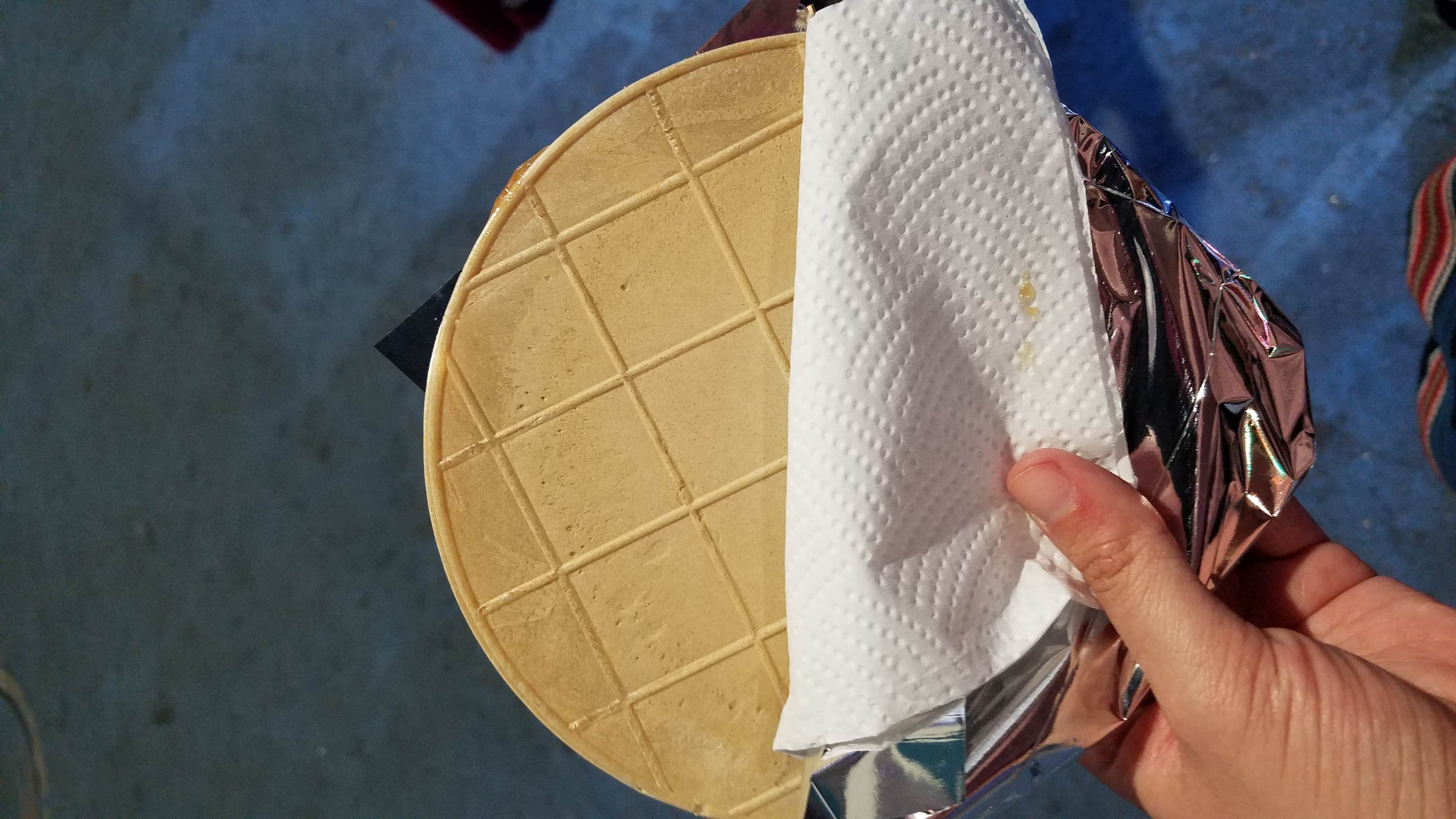
A wafer is a crisp, often sweet, very thin, flat, light biscuit, often used to decorate ice cream, and also used as a Garnish (food), garnish on some sweet dishes. They frequently have a waffle surface pattern but may also be patterned with insignia of the food's manufacturer or may be patternless. Some chocolate bars, such as Kit Kat and Toffee Crisp, are wafers with chocolate in and around them. Communion wafers A communion wafer is a type of unleavened bread consumed as part of the Christian ritual of communion. Spa wafer Special "spa wafers" (Czech: ''lázeňské oplatky'', Slovak: ''kúpeľné oblátky'') are produced in the spa towns of the Czech Republic and the Slovak Republic (e.g. Piešťany). The production of the wafers in Karlovy Vary, Karlsbad and Mariánské Lázně, Marienbad was traditional to the towns' Sudeten Germans, German-speaking population, who, after Expulsion of Germans from Czechoslovakia, the ethnic cleansing of the area, brought the craft to Germa ... [...More Info...] [...Related Items...] OR: [Wikipedia] [Google] [Baidu] |
Probe Card
A probe card (commonly referred to as a DUT board) is used in automated integrated circuit testing. It is an interface between an electronic test system and a semiconductor Wafer (electronics), wafer. Use and manufacture A probe card or DUT board is a printed circuit board, printed circuit board (PCB), and is the interface between the integrated circuit and a test head, which in turn attaches to automatic test equipment, automatic test equipment (ATE) (or "tester"). Typically, the probe card is mechanically docked to a Wafer testing prober and electrically connected to the ATE . Its purpose is to provide an electrical path between the test system and the circuits on the wafer, thereby permitting the testing and validation of the circuits at the wafer level, usually before they are diced and packaged. It normally comprises a PCB and some form of contact elements, usually metallic. A semiconductor manufacturer will typically require a new probe card for each new device wafer and ... [...More Info...] [...Related Items...] OR: [Wikipedia] [Google] [Baidu] |

