Tunnel field-effect transistor on:
[Wikipedia]
[Google]
[Amazon]
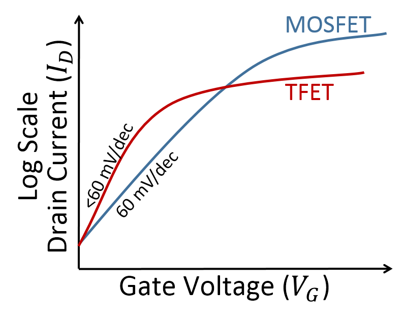
The tunnel field-effect transistor (TFET) is an experimental type of transistor. Even though its structure is very similar to a metal–oxide–semiconductor field-effect transistor ( In classical MOSFET devices, the 60 mV/decade is a fundamental limit to power scaling. The ratio between on-current and the off-current (especially the subthreshold leakage — one major contributor of power consumption) is given by the ratio between the threshold voltage and the subthreshold slope, e.g.:
:
The transistor speed is proportional to the on-current: The higher the on-current, the faster a transistor will be able to charge its fan-out (consecutive capacitive load). For a given transistor speed and a maximum acceptable subthreshold leakage, the subthreshold slope thus defines a certain minimal threshold voltage. Reducing the threshold voltage is an essential part for the idea of constant field scaling. Since 2003, the major technology developers got almost stuck in threshold voltage scaling and thus could also not scale supply voltage (which due to technical reasons has to be at least 3 times the threshold voltage for high performance devices). As a consequence, the processor speed did not develop as fast as before 2003 (see Beyond CMOS). The advent of a mass-producible TFET device with a slope far below 60 mV/decade will enable the industry to continue the scaling trends from the 1990s, where processor frequency doubled each 3 years.


MOSFET
upright=1.3, Two power MOSFETs in amperes">A in the ''on'' state, dissipating up to about 100 watt">W and controlling a load of over 2000 W. A matchstick is pictured for scale.
In electronics, the metal–oxide–semiconductor field- ...
), the fundamental switching mechanism differs, making this device a promising candidate for low power electronics
Low-power electronics are electronics designed to consume less electrical power than usual, often at some expense. For example, notebook processors usually consume less power than their desktop counterparts, at the expense of computer perform ...
. TFETs switch by modulating quantum tunneling
In physics, a quantum (: quanta) is the minimum amount of any physical entity (physical property) involved in an interaction. The fundamental notion that a property can be "quantized" is referred to as "the hypothesis of quantization". This me ...
through a barrier instead of modulating thermionic emission
Thermionic emission is the liberation of charged particles from a hot electrode whose thermal energy gives some particles enough kinetic energy to escape the material's surface. The particles, sometimes called ''thermions'' in early literature, a ...
over a barrier as in traditional MOSFETs. Because of this, TFETs are not limited by the thermal Maxwell–Boltzmann tail of carriers, which limits MOSFET drain current subthreshold swing to about 60 mV/decade
A decade (from , , ) is a period of 10 years. Decades may describe any 10-year period, such as those of a person's life, or refer to specific groupings of calendar years.
Usage
Any period of ten years is a "decade". For example, the statement ...
of current at room temperature.
TFET studies can be traced back to Stuetzer who in 1952 published first investigations of a transistor containing the basic elements of the TFET, a gated p-n junction. The reported surface conductivity control was, however, not
related to tunneling. The first TFET was reported in 1965. Joerg Appenzeller and his colleagues at IBM were the first to demonstrate that current swings below the MOSFET’s 60-mV-per-decade limit were possible. In 2004, they reported they had created a tunnel transistor with a carbon nanotube channel and a subthreshold swing of just 40 mV per decade. Theoretical work has indicated that significant power savings can be obtained by using low-voltage TFETs in place of MOSFETs in logic circuits.
 In classical MOSFET devices, the 60 mV/decade is a fundamental limit to power scaling. The ratio between on-current and the off-current (especially the subthreshold leakage — one major contributor of power consumption) is given by the ratio between the threshold voltage and the subthreshold slope, e.g.:
:
The transistor speed is proportional to the on-current: The higher the on-current, the faster a transistor will be able to charge its fan-out (consecutive capacitive load). For a given transistor speed and a maximum acceptable subthreshold leakage, the subthreshold slope thus defines a certain minimal threshold voltage. Reducing the threshold voltage is an essential part for the idea of constant field scaling. Since 2003, the major technology developers got almost stuck in threshold voltage scaling and thus could also not scale supply voltage (which due to technical reasons has to be at least 3 times the threshold voltage for high performance devices). As a consequence, the processor speed did not develop as fast as before 2003 (see Beyond CMOS). The advent of a mass-producible TFET device with a slope far below 60 mV/decade will enable the industry to continue the scaling trends from the 1990s, where processor frequency doubled each 3 years.
Structure
The basic TFET structure is similar to a MOSFET except that the source and drain terminals of a TFET are doped of opposite types (see figure). A common TFET device structure consists of a P-I-N ( p-type,intrinsic
In science and engineering, an intrinsic property is a property of a specified subject that exists itself or within the subject. An extrinsic property is not essential or inherent to the subject that is being characterized. For example, mass i ...
, n-type) junction, in which the electrostatic potential of the intrinsic region is controlled by a gate
A gate or gateway is a point of entry to or from a space enclosed by walls. The word is derived from Proto-Germanic language, Proto-Germanic ''*gatan'', meaning an opening or passageway. Synonyms include yett (which comes from the same root w ...
terminal.

Device operation
The device is operated by applying gate bias so that electron accumulation occurs in the intrinsic region for an n-type TFET. At sufficient gate bias, band-to-band tunneling (BTBT) occurs when theconduction band
In solid-state physics, the valence band and conduction band are the bands closest to the Fermi level, and thus determine the electrical conductivity of the solid. In nonmetals, the valence band is the highest range of electron energies in ...
of the intrinsic region aligns with the valence band
In solid-state physics, the valence band and conduction band are the bands closest to the Fermi level, and thus determine the electrical conductivity of the solid. In nonmetals, the valence band is the highest range of electron energies in ...
of the P region. Electrons from the valence band of the p-type region tunnel into the conduction band of the intrinsic region and current can flow across the device. As the gate bias is reduced, the bands become misaligned and current can no longer flow.

Prototype devices
A group at IBM were the first to demonstrate that current swings below the MOSFET’s 60-mV-per-decade limit were possible. In 2004, they reported a tunnel transistor with acarbon nanotube
A carbon nanotube (CNT) is a tube made of carbon with a diameter in the nanometre range ( nanoscale). They are one of the allotropes of carbon. Two broad classes of carbon nanotubes are recognized:
* ''Single-walled carbon nanotubes'' (''S ...
channel and a subthreshold swing of just 40 mV per decade.
By 2010, many TFETs have been fabricated in different material systems, but none has yet been able to demonstrate steep subthreshold slope at drive currents required for mainstream applications. In IEDM' 2016, a group from Lund University demonstrated a vertical nanowire InAs/ GaAsSb/ GaSb TFET, which exhibits a subthreshold swing of 48 mV/decade, a on-current of 10.6 μA/μm for off-current of 1 nA/μm at a supply voltage of 0.3 V, showing the potential of outperforming Si MOSFETs at a supply voltage lower than 0.3 V.
Theory and simulations
Double-gate thin-body quantum well-to-quantum well TFET structures have been proposed to overcome some challenges associated with the lateral TFET structure, such as its requirement for ultra sharp doping profiles; however, such devices may be plagued by gate leakage due to large vertical fields in the device structure. Simulations in 2013 showed that TFETs using InAs-GaSb may have a subthreshold swing of 33 mV/decade under ideal conditions. The use of van der Waals heterostructures for TFETs were proposed in 2016.See also
*Tunnel junction
In electronics, a tunnel junction is a barrier, such as a thin insulating layer or electric potential, between two electrically conducting materials. Electrons (or quasiparticles) pass through the barrier by the process of quantum tunnelling. Clas ...
*Tunnel diode
A tunnel diode or Esaki diode is a type of semiconductor diode that has effectively " negative resistance" due to the quantum mechanical effect called tunneling. It was invented in August 1957 by Leo Esaki and Yuriko Kurose when working ...
*Carver Mead
Carver Andress Mead (born 1 May 1934) is an American scientist and engineer. He currently holds the position of Gordon and Betty Moore Professor Emeritus of Engineering and Applied Science at the California Institute of Technology (Caltech), ...
References
{{Authority control Transistor types Field-effect transistors