|
Nanoelectromechanical Systems
Nanoelectromechanical systems (NEMS) are a class of devices integrating electrical and mechanical functionality on the nanoscale. NEMS form the next logical miniaturization step from so-called microelectromechanical systems, or MEMS devices. NEMS typically integrate transistor-like nanoelectronics with mechanical actuators, pumps, or motors, and may thereby form physical, biological, and chemical sensors. The name derives from typical device dimensions in the nanometer range, leading to low mass, high mechanical resonance frequencies, potentially large quantum mechanical effects such as zero point motion, and a high surface-to-volume ratio useful for surface-based sensing mechanisms. Applications include accelerometers and sensors to detect chemical substances in the air. History Background As noted by Richard Feynman in his famous talk in 1959, " There's Plenty of Room at the Bottom," there are many potential applications of machines at smaller and smaller sizes; by building ... [...More Info...] [...Related Items...] OR: [Wikipedia] [Google] [Baidu] |
Gate Oxide
The gate oxide is the dielectric layer that separates the gate terminal of a MOSFET (metal-oxide-semiconductor field-effect transistor) from the underlying source and drain terminals as well as the conductive channel that connects source and drain when the transistor is turned on. Gate oxide is formed by thermal oxidation of the silicon of the channel to form a thin (5 - 200 nm) insulating layer of silicon dioxide. The insulating silicon dioxide layer is formed through a process of self-limiting oxidation, which is described by the Deal–Grove model. A conductive gate material is subsequently deposited over the gate oxide to form the transistor. The gate oxide serves as the dielectric layer so that the gate can sustain as high as 1 to 5 MV/cm transverse electric field in order to strongly modulate the conductance of the channel. Above the gate oxide is a thin electrode layer made of a conductor which can be aluminium, a highly doped silicon, a refractory metal such as tun ... [...More Info...] [...Related Items...] OR: [Wikipedia] [Google] [Baidu] |
FinFET
A fin field-effect transistor (FinFET) is a multigate device, a MOSFET (metal-oxide-semiconductor field-effect transistor) built on a substrate where the gate is placed on two, three, or four sides of the channel or wrapped around the channel, forming a double or even multi gate structure. These devices have been given the generic name "FinFETs" because the source/drain region forms fins on the silicon surface. The FinFET devices have significantly faster switching times and higher current density than planar CMOS (complementary metal-oxide-semiconductor) technology. FinFET is a type of non-planar transistor, or "3D" transistor. It is the basis for modern nanoelectronic semiconductor device fabrication. Microchips utilizing FinFET gates first became commercialized in the first half of the 2010s, and became the dominant gate design at 14 nm, 10 nm and 7 nm process nodes. It is common for a single FinFET transistor to contain several fins, arranged side by side and all cove ... [...More Info...] [...Related Items...] OR: [Wikipedia] [Google] [Baidu] |
20 nm
NM, nm, and variations may refer to: Businesses and organizations * Northwestern Mutual, financial services company in Wisconsin, United States * Air Madrid (IATA airline designator NM), Spanish airline * Mount Cook Airline (IATA airline designator NM), New Zealand airline * Manx2 (IATA airline designator NM), Isle of Man airline Places * The National Mall in Washington, D.C., United States * Navi Mumbai, India * New Mexico, a state of the United States (postal abbreviation) * Inner Mongolia, an autonomous region of China (Guobiao abbreviation and ISO-3166-2:CN code NM) Science and technology Medicine * Nemaline myopathy, a neuromuscular disorder * Neuromelanin, a dark pigment found in the brain * Nuclear medicine, a medical imaging modality Units of measure * Nanometer (nm), an SI unit of length, equal to 10−9 m (a thousand-millionth of a meter) * Nanomolar (nM), in chemistry, one thousand-millionth molar * Nautical mile (NM or nmi), a unit of leng ... [...More Info...] [...Related Items...] OR: [Wikipedia] [Google] [Baidu] |
MOSFET Scaling
The metal–oxide–semiconductor field-effect transistor (MOSFET, MOS-FET, or MOS FET) is a type of field-effect transistor (FET), most commonly fabricated by the controlled oxidation of silicon. It has an insulated gate, the voltage of which determines the conductivity of the device. This ability to change conductivity with the amount of applied voltage can be used for amplifying or switching electronic signals. A metal-insulator-semiconductor field-effect transistor (MISFET) is a term almost synonymous with MOSFET. Another synonym is IGFET for insulated-gate field-effect transistor. The basic principle of the field-effect transistor was first patented by Julius Edgar Lilienfeld in 1925.Lilienfeld, Julius Edgar (1926-10-08) "Method and apparatus for controlling electric currents" upright=1.6, Two power MOSFETs in watt.html" ;"title="amperes">A in the ''on'' state, dissipating up to about 100 watt">W and controlling a load of over 2000 W. A matchstick is pictured ... [...More Info...] [...Related Items...] OR: [Wikipedia] [Google] [Baidu] |
Multigate Device
A multigate device, multi-gate MOSFET or multi-gate field-effect transistor (MuGFET) refers to a metal–oxide–semiconductor field-effect transistor (MOSFET) that has more than one gate on a single transistor. The multiple gates may be controlled by a single gate electrode, wherein the multiple gate surfaces act electrically as a single gate, or by independent gate electrodes. A multigate device employing independent gate electrodes is sometimes called a multiple-independent-gate field-effect transistor (MIGFET). The most widely used multi-gate devices are the FinFET (fin field-effect transistor) and the GAAFET (gate-all-around field-effect transistor), which are non-planar transistors, or 3D transistors. Multi-gate transistors are one of the several strategies being developed by MOS semiconductor manufacturers to create ever-smaller microprocessors and memory cells, colloquially referred to as extending Moore's law (in its narrow, specific version concerning density scaling ... [...More Info...] [...Related Items...] OR: [Wikipedia] [Google] [Baidu] |
Bijan Davari
Bijan Davari (born September 16, 1954) is an Iranian-American engineer. He is an IBM Fellow and Vice President at IBM Thomas J Watson Research Center, Yorktown Hts, NY. His pioneering work in the miniaturization of semiconductor devices changed the world of computing. His research led to the first generation of voltage-scaled deep-submicron CMOS with sufficient performance to totally replace bipolar technology in IBM mainframes and enable new high-performance UNIX servers. As head of IBM’s Semiconductor Research Center (SRDC), he led IBM into the use of Copper interconnect, silicon on insulator (SOI), and Embedded DRAM before its rivals. He is a member of the U.S. National Academy of Engineering and is known for his seminal contributions to the field of CMOS technology. He is an IEEE Fellow, recipient of the J J Ebers Award in 2005 and IEEE Andrew S. Grove Award in 2010. At the present time, he leads the Next Generation Systems Area of research. Education Bijan Davari was b ... [...More Info...] [...Related Items...] OR: [Wikipedia] [Google] [Baidu] |
CRC Press
The CRC Press, LLC is an American publishing group that specializes in producing technical books. Many of their books relate to engineering, science and mathematics. Their scope also includes books on business, forensics and information technology. CRC Press is now a division of Taylor & Francis, itself a subsidiary of Informa. History The CRC Press was founded as the Chemical Rubber Company (CRC) in 1903 by brothers Arthur, Leo and Emanuel Friedman in Cleveland, Ohio, based on an earlier enterprise by Arthur, who had begun selling rubber laboratory aprons in 1900. The company gradually expanded to include sales of laboratory equipment to chemists. In 1913 the CRC offered a short (116-page) manual called the ''Rubber Handbook'' as an incentive for any purchase of a dozen aprons. Since then the ''Rubber Handbook'' has evolved into the CRC's flagship book, the ''CRC Handbook of Chemistry and Physics''. In 1964, Chemical Rubber decided to focus on its publishing ventures ... [...More Info...] [...Related Items...] OR: [Wikipedia] [Google] [Baidu] |
10 nm
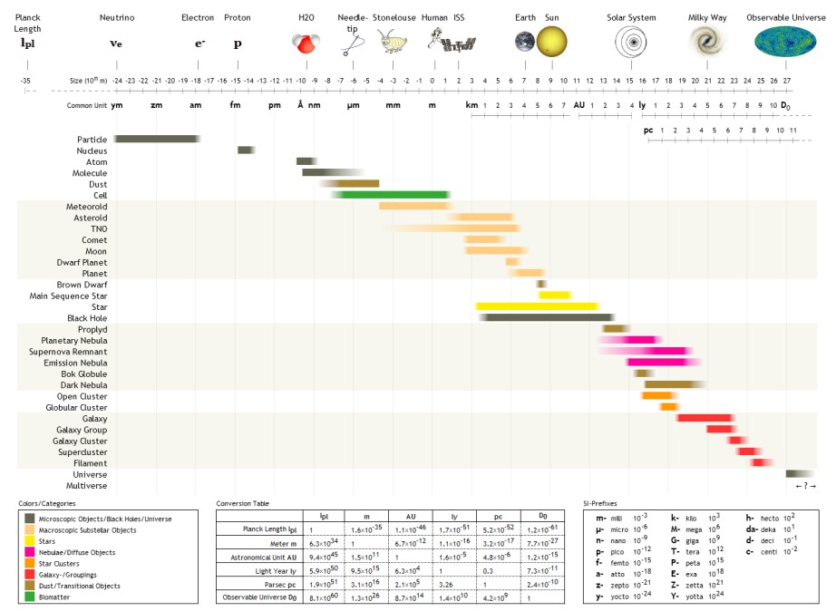
The following are examples of orders of magnitude for different lengths. __TOC__ Overview Detailed list To help compare different orders of magnitude, the following list describes various lengths between 1.6 \times 10^ metres and 10^metres. Subatomic scale Atomic to cellular scale Cellular to human scale Human to astronomical scale Astronomical scale Less than 1 zeptometre The ' ( SI symbol: ') is a unit of length in the metric system equal to . To help compare different orders of magnitude, this section lists lengths shorter than 10−21 m (1 zm). *1.6 × 10⁻⁵ quectometres (1.6 × 10⁻³⁵ metres) – the Planck length (Measures of distance shorter than this do not make physical sense, according to current theories of physics.) *1 qm – 1 quectometre, the smallest named subdivision of the metre in the SI base unit of length, one nonillionth of a metre *1 rm – 1 rontometre, a subdivision of the metre in the SI base unit of length, one octilliont ... [...More Info...] [...Related Items...] OR: [Wikipedia] [Google] [Baidu] |
Thin Films
A thin film is a layer of material ranging from fractions of a nanometer ( monolayer) to several micrometers in thickness. The controlled synthesis of materials as thin films (a process referred to as deposition) is a fundamental step in many applications. A familiar example is the household mirror, which typically has a thin metal coating on the back of a sheet of glass to form a reflective interface. The process of silvering was once commonly used to produce mirrors, while more recently the metal layer is deposited using techniques such as sputtering. Advances in thin film deposition techniques during the 20th century have enabled a wide range of technological breakthroughs in areas such as magnetic recording media, electronic semiconductor devices, integrated passive devices, LEDs, optical coatings (such as antireflective coatings), hard coatings on cutting tools, and for both energy generation (e.g. thin-film solar cells) and storage ( thin-film batteries). It is al ... [...More Info...] [...Related Items...] OR: [Wikipedia] [Google] [Baidu] |
Gold
Gold is a chemical element with the symbol Au (from la, aurum) and atomic number 79. This makes it one of the higher atomic number elements that occur naturally. It is a bright, slightly orange-yellow, dense, soft, malleable, and ductile metal in a pure form. Chemically, gold is a transition metal and a group 11 element. It is one of the least reactive chemical elements and is solid under standard conditions. Gold often occurs in free elemental (native state), as nuggets or grains, in rocks, veins, and alluvial deposits. It occurs in a solid solution series with the native element silver (as electrum), naturally alloyed with other metals like copper and palladium, and mineral inclusions such as within pyrite. Less commonly, it occurs in minerals as gold compounds, often with tellurium ( gold tellurides). Gold is resistant to most acids, though it does dissolve in aqua regia (a mixture of nitric acid and hydrochloric acid), forming a soluble tetrachloroau ... [...More Info...] [...Related Items...] OR: [Wikipedia] [Google] [Baidu] |
Transistor
upright=1.4, gate (G), body (B), source (S) and drain (D) terminals. The gate is separated from the body by an insulating layer (pink). A transistor is a semiconductor device used to Electronic amplifier, amplify or electronic switch, switch electrical signals and electrical power, power. The transistor is one of the basic building blocks of modern electronics. It is composed of semiconductor material, usually with at least three terminals for connection to an electronic circuit. A voltage or current applied to one pair of the transistor's terminals controls the current through another pair of terminals. Because the controlled (output) power can be higher than the controlling (input) power, a transistor can amplify a signal. Some transistors are packaged individually, but many more are found embedded in integrated circuits. Austro-Hungarian physicist Julius Edgar Lilienfeld proposed the concept of a field-effect transistor in 1926, but it was not possible to actually co ... [...More Info...] [...Related Items...] OR: [Wikipedia] [Google] [Baidu] |


_250_nm_by_250_nm_image_of_one-atom-thick_silver_islands_grown_on_palladium_(111)_surface.png)

.jpg)