|
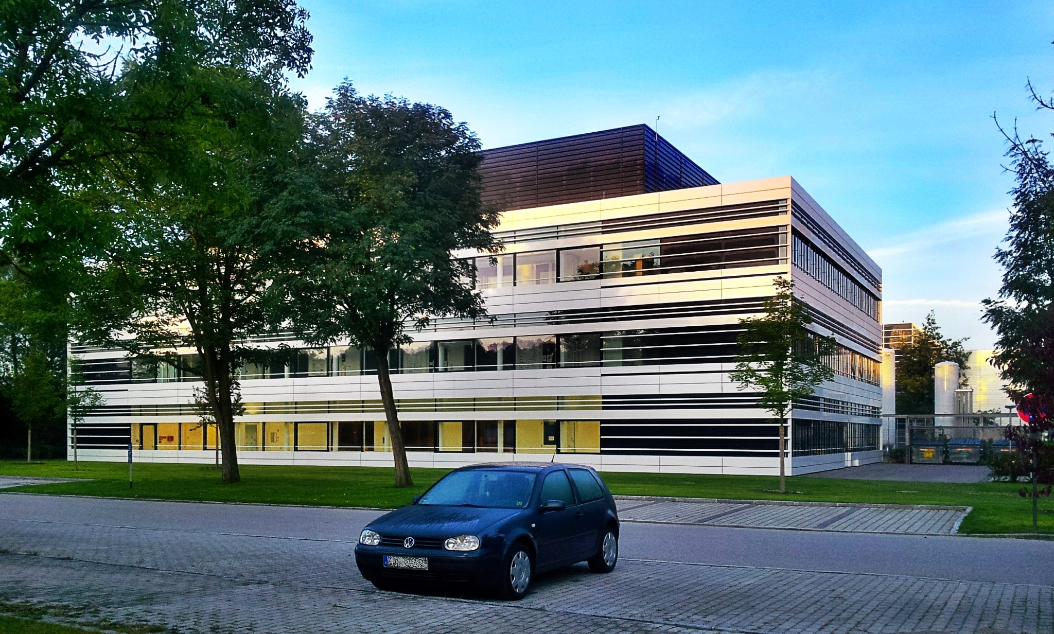
Walter Schottky Institute
The Walter Schottky Institute (WSI) (german: Walter-Schottky-Institut) is a research center at the Technical University of Munich, dedicated to the physics of semiconductors. Established in 1988, it is located on its Garching campus. It is named after physicist Walter H. Schottky. History The idea for an interdisciplinary research facility that would bridge the gap between fundamental physics and applied semiconductor electronics emerged in the early 1980s. In February 1985, Gerhard Abstreiter, professor at the Technical University of Munich, wrote a memorandum about the establishment of a research institute, with specific focus on semiconductor research and device development. After Klaus von Klitzing, who had been working at the physics department of the TU Munich until shortly before the announcement, was awarded the Nobel Prize in Physics in 1985, the idea, which was already supported by the research board of Siemens, received great approval. Thus, as early as December ... [...More Info...] [...Related Items...] OR: [Wikipedia] [Google] [Baidu] |
Garching
Garching bei München (''Garching near Munich'') or Garching is a town in Bavaria, Germany, near Munich. It is the home of several research institutes and university departments on its campus. It became a city on 14 September 1990. Location The town is at , near the river Isar and the Bundesautobahn 9. Garching has a number of scientific research institutes and scientific experiment facilities located in the city, including a linear accelerator and a research nuclear reactor. The nuclear research reactor, nicknamed ''Atomei'' (atomic egg) appears in the city's coat of arms, and started the process leading to an accumulation of research institutes. A number of roads and places in the city are named after scientists, mathematicians and technical innovators such as Carl von Linde, Rudolf Diesel, Albert Einstein, Leonhard Euler, Werner Heisenberg, Max Planck, Wilhelm Röntgen, and Erwin Schrödinger. Districts The town has four districts: * Garching * Dirnismaning * Hochbrück * H ... [...More Info...] [...Related Items...] OR: [Wikipedia] [Google] [Baidu] |
TUM Department Of Physics
The TUM School of Natural Sciences (NAT) is a school of the Technical University of Munich, established in 2022 by the merger of various former departments. As of 2022, it is structured into the Department of Biosciences, the Department of Chemistry, and the Department of Physics. The school is located at the TUM Campus Garching, Garching campus. Department of Chemistry History Chairs As of 2020, the department consists of 24 chairs and institutes: * Analytical chemistry, Analytical Chemistry and Water Chemistry * Inorganic chemistry, Inorganic Chemistry * Inorganic and Organometallic chemistry, Organometallic Chemistry * Inorganic Chemistry with Focus on New Materials * Construction Chemistry * Construction Chemicals * Biochemistry * Biomolecular Nuclear magnetic resonance spectroscopy, NMR-Spectroscopy * Biophysical chemistry, Biophysical Chemistry * Biotechnology * Food chemistry, Food Chemistry * Macromolecule, Macromolecular Chemistry * Medicinal chemistry, Medicinal ... [...More Info...] [...Related Items...] OR: [Wikipedia] [Google] [Baidu] |
Research Institutes In Germany
Research is " creative and systematic work undertaken to increase the stock of knowledge". It involves the collection, organization and analysis of evidence to increase understanding of a topic, characterized by a particular attentiveness to controlling sources of bias and error. These activities are characterized by accounting and controlling for biases. A research project may be an expansion on past work in the field. To test the validity of instruments, procedures, or experiments, research may replicate elements of prior projects or the project as a whole. The primary purposes of basic research (as opposed to applied research) are documentation, discovery, interpretation, and the research and development (R&D) of methods and systems for the advancement of human knowledge. Approaches to research depend on epistemologies, which vary considerably both within and between humanities and sciences. There are several forms of research: scientific, humanities, artistic, econom ... [...More Info...] [...Related Items...] OR: [Wikipedia] [Google] [Baidu] |
Nanoelectronics
Nanoelectronics refers to the use of nanotechnology in electronic components. The term covers a diverse set of devices and materials, with the common characteristic that they are so small that inter-atomic interactions and quantum mechanical properties need to be studied extensively. Some of these candidates include: hybrid molecular/semiconductor electronics, one-dimensional nanotubes/nanowires (e.g. silicon nanowires or carbon nanotubes) or advanced molecular electronics. Nanoelectronic devices have critical dimensions with a size range between 1 nm and 100 nm. Recent silicon MOSFET (metal-oxide-semiconductor field-effect transistor, or MOS transistor) technology generations are already within this regime, including 22 nanometers CMOS (complementary MOS) nodes and succeeding 14 nm, 10 nm and 7 nm FinFET (fin field-effect transistor) generations. Nanoelectronics is sometimes considered as disruptive technology because present candidates are significantly different f ... [...More Info...] [...Related Items...] OR: [Wikipedia] [Google] [Baidu] |
Molecular-beam Epitaxy
Molecular-beam epitaxy (MBE) is an epitaxy method for thin-film deposition of single crystals. MBE is widely used in the manufacture of semiconductor devices, including transistors, and it is considered one of the fundamental tools for the development of nanotechnologies. MBE is used to fabricate diodes and MOSFETs (MOS field-effect transistors) at microwave frequencies, and to manufacture the lasers used to read optical discs (such as CDs and DVDs). History Original ideas of MBE process were first established by Günther. Films he deposited were not epitaxial, but were deposited on glass substrates. With the development of vacuum technology, MBE process was demonstrated by Davey and Pankey who succeeded in growing GaAs epitaxial films on single crystal GaAs substrates using Günther's method. Major subsequent development of MBE films was enabled by J.R. Arthur's investigations of kinetic behavior of growth mechanisms and Alfred Y. Cho's in situ observation of MBE process usin ... [...More Info...] [...Related Items...] OR: [Wikipedia] [Google] [Baidu] |
Cleanroom
A cleanroom or clean room is an engineered space, which maintains a very low concentration of airborne particulates. It is well isolated, well-controlled from contamination, and actively cleansed. Such rooms are commonly needed for scientific research, and in industrial production for all nanoscale processes, such as semiconductor manufacturing. A cleanroom is designed to keep everything from dust, to airborne organisms, or vaporised particles, away from it, and so from whatever material is being handled inside it. The other way around, a cleanroom can also help keep materials escaping from it. This is often the primary aim in hazardous biology and nuclear work, in pharmaceutics and in virology. Cleanrooms typically come with a cleanliness level quantified by the number of particles per cubic meter at a predetermined molecule measure. The ambient outdoor air in a typical urban area contains 35,000,000 particles for each cubic meter in the size range 0.5 μm and bigger, equ ... [...More Info...] [...Related Items...] OR: [Wikipedia] [Google] [Baidu] |
Siemens
Siemens AG ( ) is a German multinational conglomerate corporation and the largest industrial manufacturing company in Europe headquartered in Munich with branch offices abroad. The principal divisions of the corporation are ''Industry'', ''Energy'', ''Healthcare'' (Siemens Healthineers), and ''Infrastructure & Cities'', which represent the main activities of the corporation. The corporation is a prominent maker of medical diagnostics equipment and its medical health-care division, which generates about 12 percent of the corporation's total sales, is its second-most profitable unit, after the industrial automation division. In this area, it is regarded as a pioneer and the company with the highest revenue in the world. The corporation is a component of the Euro Stoxx 50 stock market index. Siemens and its subsidiaries employ approximately 303,000 people worldwide and reported global revenue of around €62 billion in 2021 according to its earnings release. History 1847 to ... [...More Info...] [...Related Items...] OR: [Wikipedia] [Google] [Baidu] |
Nobel Prize In Physics
) , image = Nobel Prize.png , alt = A golden medallion with an embossed image of a bearded man facing left in profile. To the left of the man is the text "ALFR•" then "NOBEL", and on the right, the text (smaller) "NAT•" then "MDCCCXXXIII" above, followed by (smaller) "OB•" then "MDCCCXCVI" below. , awarded_for = Outstanding contributions for humankind in the field of Physics , presenter = Royal Swedish Academy of Sciences , location = Stockholm, Sweden , date = , reward = 9 million Swedish kronor (2017) , year = 1901 , holder_label = Most recently awarded to , holder = Alain Aspect, John Clauser, and Anton Zeilinger , most_awards = John Bardeen (2) , website nobelprize.org, previous = 2021 , year2=2022, main=2022, next=2023 The Nobel Prize in Physics is a yearly award given by the Royal Swedish Academy of Sciences for those who have made the most outstanding contributions for humankind in the field of physics. It ... [...More Info...] [...Related Items...] OR: [Wikipedia] [Google] [Baidu] |
Klaus Von Klitzing
Klaus von Klitzing (, born 28 June 1943, Schroda) is a German physicist, known for discovery of the integer quantum Hall effect, for which he was awarded the 1985 Nobel Prize in Physics. Education In 1962, Klitzing passed the Abitur at the Artland-Gymnasium in Quakenbrück, Germany, before studying physics at the Braunschweig University of Technology, where he received his diploma in 1969. He continued his studies at the University of Würzburg at the chair of Gottfried Landwehr, completing his PhD thesis entitled ''Galvanomagnetic Properties of Tellurium in Strong Magnetic Fields'' in 1972, and gaining habilitation in 1978. Research and career During his career Klitzing has worked at the Clarendon Laboratory at the University of Oxford and the Grenoble High Magnetic Field Laboratory in France (now LNCMI), where he continued to work until becoming a professor at the Technical University of Munich in 1980. He has been a director of the Max Planck Institute for Solid State Rese ... [...More Info...] [...Related Items...] OR: [Wikipedia] [Google] [Baidu] |
Semiconductor Physics
A semiconductor is a material which has an electrical conductivity value falling between that of a conductor, such as copper, and an insulator, such as glass. Its resistivity falls as its temperature rises; metals behave in the opposite way. Its conducting properties may be altered in useful ways by introducing impurities (" doping") into the crystal structure. When two differently doped regions exist in the same crystal, a semiconductor junction is created. The behavior of charge carriers, which include electrons, ions, and electron holes, at these junctions is the basis of diodes, transistors, and most modern electronics. Some examples of semiconductors are silicon, germanium, gallium arsenide, and elements near the so-called "metalloid staircase" on the periodic table. After silicon, gallium arsenide is the second-most common semiconductor and is used in laser diodes, solar cells, microwave-frequency integrated circuits, and others. Silicon is a critical element for fabrica ... [...More Info...] [...Related Items...] OR: [Wikipedia] [Google] [Baidu] |
Gerhard Abstreiter
Gerhard Abstreiter is a German physicist and professor of physics at Technical University of Munich (TUM), currently holding the university's highest honor, the Emeritus of Excellence and also being a distinguished visiting professor at University of California, Santa Barbara. From 1987 to 2015, he was a full professor at TUM and also, in 2010 and 2011, a distinguished visiting professor at University of Tokyo. He is a Fellow of the American Physical Society, Bavarian Academy of Sciences and Humanities and acatech. He won the Max Born Medal and Prize The Max Born Medal and Prize is a scientific prize awarded yearly by the German Physical Society (DPG) and the British Institute of Physics (IOP) in memory of the German physicist Max Born, who was a German-Jewish physicist, instrumental in the ... in 1998. References Year of birth missing (living people) Living people Academic staff of the Technical University of Munich 21st-century German physicists Fellows of the Am ... [...More Info...] [...Related Items...] OR: [Wikipedia] [Google] [Baidu] |


.jpg)
