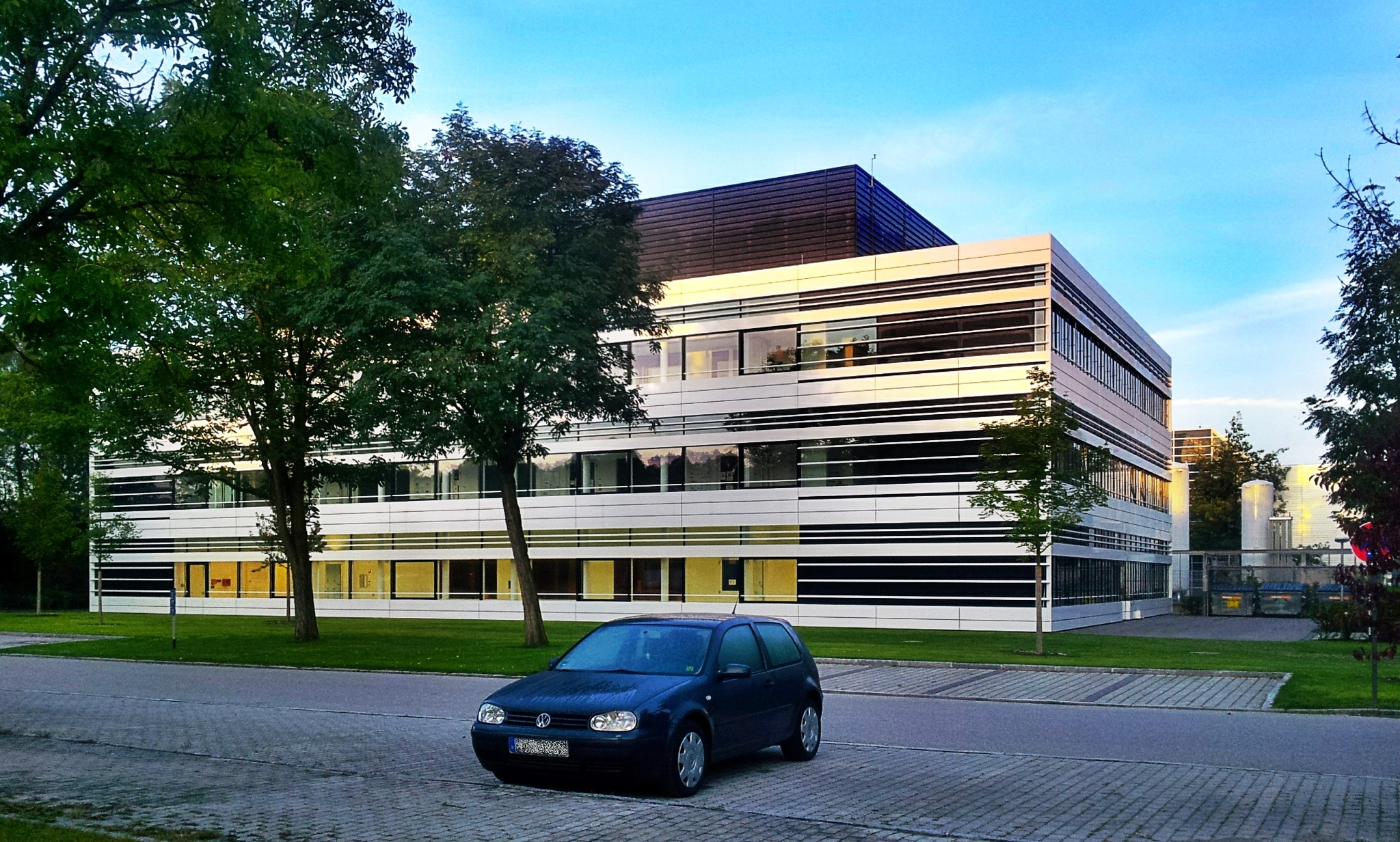
Walter Schottky Institute on:
[Wikipedia]
[Google]
[Amazon]
The Walter Schottky Institute (WSI) (german: Walter-Schottky-Institut) is a
 The institute building covers an area of 2400 m2 and provides space for laboratories and offices of eight research groups in four chairs with a total of over 150 employees. Of this, 250 m2 is available as a
research center
Center or centre may refer to:
Mathematics
*Center (geometry), the middle of an object
* Center (algebra), used in various contexts
** Center (group theory)
** Center (ring theory)
* Graph center, the set of all vertices of minimum eccentricit ...
at the Technical University of Munich
The Technical University of Munich (TUM or TU Munich; german: Technische Universität München) is a public research university in Munich, Germany. It specializes in engineering, technology, medicine, and applied and natural sciences.
Establis ...
, dedicated to the physics
Physics is the natural science that studies matter, its fundamental constituents, its motion and behavior through space and time, and the related entities of energy and force. "Physical science is that department of knowledge which r ...
of semiconductor
A semiconductor is a material which has an electrical conductivity value falling between that of a conductor, such as copper, and an insulator, such as glass. Its resistivity falls as its temperature rises; metals behave in the opposite way. ...
s. Established in 1988, it is located on its Garching campus. It is named after physicist Walter H. Schottky
Walter Hans Schottky (23 July 1886 – 4 March 1976) was a German physicist who played a major early role in developing the theory of electron and ion emission phenomena, invented the screen-grid vacuum tube in 1915 while working at Siemens ...
.
History
The idea for an interdisciplinary research facility that would bridge the gap between fundamentalphysics
Physics is the natural science that studies matter, its fundamental constituents, its motion and behavior through space and time, and the related entities of energy and force. "Physical science is that department of knowledge which r ...
and applied semiconductor electronics
A semiconductor device is an electronic component that relies on the electronic properties of a semiconductor material (primarily silicon, germanium, and gallium arsenide, as well as organic semiconductors) for its function. Its conductivity li ...
emerged in the early 1980s. In February 1985, Gerhard Abstreiter, professor at the Technical University of Munich
The Technical University of Munich (TUM or TU Munich; german: Technische Universität München) is a public research university in Munich, Germany. It specializes in engineering, technology, medicine, and applied and natural sciences.
Establis ...
, wrote a memorandum about the establishment of a research institute, with specific focus on semiconductor research and device development. After Klaus von Klitzing
Klaus von Klitzing (, born 28 June 1943, Schroda) is a German physicist, known for discovery of the integer quantum Hall effect, for which he was awarded the 1985 Nobel Prize in Physics.
Education
In 1962, Klitzing passed the Abitur at the A ...
, who had been working at the physics department of the TU Munich until shortly before the announcement, was awarded the Nobel Prize in Physics
)
, image = Nobel Prize.png
, alt = A golden medallion with an embossed image of a bearded man facing left in profile. To the left of the man is the text "ALFR•" then "NOBEL", and on the right, the text (smaller) "NAT•" then " ...
in 1985, the idea, which was already supported by the research board of Siemens, received great approval.
Thus, as early as December 1985, the general conditions for founding the research institute as a collaborative project between the Technical University of Munich and Siemens were discussed with Bavarian state government. The construction costs were paid jointly by Siemens and the Bavarian state. After two years of construction, the Walter Schottky Institute was officially inaugurated on July 14, 1988. The university took over the institute completely in 1992.
Facilities
 The institute building covers an area of 2400 m2 and provides space for laboratories and offices of eight research groups in four chairs with a total of over 150 employees. Of this, 250 m2 is available as a
 cleanroom
A cleanroom or clean room is an engineered space, which maintains a very low concentration of airborne particulates. It is well isolated, well-controlled from contamination, and actively cleansed. Such rooms are commonly needed for scientif ...
. The equipment includes several molecular-beam epitaxy
Molecular-beam epitaxy (MBE) is an epitaxy method for thin-film deposition of single crystals. MBE is widely used in the manufacture of semiconductor devices, including transistors, and it is considered one of the fundamental tools for the develo ...
systems, which are used to fabricate nanoelectronic
Nanoelectronics refers to the use of nanotechnology in electronic components. The term covers a diverse set of devices and materials, with the common characteristic that they are so small that inter-atomic interactions and quantum mechanical pr ...
structures. The institute is considered one of the world's leading research facilities for the fabrication and characterization of semiconductor heterostructures.
In July 2010, an extension building, the ''Center for Nanotechnology and Nanoscience'', was opened in the immediate vicinity.
References
Technical University of Munich Research institutes in Germany 1986 establishments in Germany Research institutes established in 1986 {{sci-org-stub