|
Ultratech
Ultratech, Inc. is an international technology company based in San Jose, California, that supplies equipment to global semiconductor fabrication plants, and also makes tools for nanotechnology applications by optical networking, data storage and automotive and display industries. Since May 2017 it has been owned by Veeco. History 1980s Ultratech Stepper, Inc., was founded in 1979 by Leo de Bos, located in Santa Clara, California. The product line consisted of 1x microlithography steppers, using a unique catadioptric lens design. Until 1992, Ultratech Stepper, Inc., was a subsidiary of General Signal. Previous presidents included Leo de Bos and George Rutland. In 1986, Drytek was sold to General Signal Technology Corp. Zafiropoulo remained on as President and CEO of the Drytek subsidiary with General Signal. 1990s In September 1992, Zafiropoulo reformed Ultratech Stepper, as a separate company, to acquire certain assets and liabilities of the Ultratech Stepper Division of General ... [...More Info...] [...Related Items...] OR: [Wikipedia] [Google] [Baidu] |
Veeco
Veeco is a global capital equipment supplier, headquartered in the U.S., that designs and builds processing systems used in semiconductor A semiconductor is a material which has an electrical conductivity value falling between that of a conductor, such as copper, and an insulator, such as glass. Its resistivity falls as its temperature rises; metals behave in the opposite way. ... and compound semiconductor manufacturing, Data Storage Technology, data storage and scientific markets for applications such as Advanced packaging (semiconductors), advanced packaging, photonics, power electronics and display technologies. Veeco's processing system capabilities include laser annealing, photolithography, ion beam etch and deposition, Metalorganic vapour-phase epitaxy, metal organic chemical vapor deposition (MOCVD), wet wafer processing, molecular beam epitaxy (MBE), atomic layer deposition (ALD), physical vapor deposition (PVD), dicing and lapping, and gas and vapor delivery. T ... [...More Info...] [...Related Items...] OR: [Wikipedia] [Google] [Baidu] |
ASML Holding
ASML Holding N.V. (commonly shortened to ASML, originally standing for Advanced Semiconductor Materials Lithography) is a Dutch multinational corporation founded in 1984. ASML specializes in the development and manufacturing of photolithography machines which are used to produce computer chips. it is the largest supplier for the semiconductor industry and the sole supplier in the world of extreme ultraviolet lithography (EUV) photolithography machines used to manufacture the most advanced chips. As of 2022, ASML was the most highly valued European tech company by market capitalization with about $200 billion. Products ASML produces the photolithography machines used in the production of computer chips. In these machines, patterns are optically imaged onto a silicon wafer that is covered with a film of light-sensitive material (photoresist). This procedure is repeated dozens of times on a single wafer. The photoresist is then further processed to create the actual electronic ci ... [...More Info...] [...Related Items...] OR: [Wikipedia] [Google] [Baidu] |
Photolithography
In integrated circuit manufacturing, photolithography or optical lithography is a general term used for techniques that use light to produce minutely patterned thin films of suitable materials over a substrate, such as a silicon wafer, to protect selected areas of it during subsequent etching, deposition, or implantation operations. Typically, ultraviolet light is used to transfer a geometric design from an optical mask to a light-sensitive chemical (photoresist) coated on the substrate. The photoresist either breaks down or hardens where it is exposed to light. The patterned film is then created by removing the softer parts of the coating with appropriate solvents. Conventional photoresists typically consists of three components: resin, sensitizer, and solvent. Photolithography processes can be classified according to the type of light used, such as ultraviolet, deep ultraviolet, extreme ultraviolet, or X-ray. The wavelength of light used determines the minimum feature si ... [...More Info...] [...Related Items...] OR: [Wikipedia] [Google] [Baidu] |
Equipment Semiconductor Companies
Equipment most commonly refers to a set of tools or other objects commonly used to achieve a particular objective. Different job Work or labor (or labour in British English) is intentional activity people perform to support the needs and wants of themselves, others, or a wider community. In the context of economics, work can be viewed as the human activity that contr ...s require different kinds of equipment.Steven Nahmias, Tava Lennon Olsen, ''Production and Operations Analysis: Seventh Edition'' (2015), p. 490. Types of equipment Types of equipment include: See also * * * * :Equipment References {{Tool-stub ... [...More Info...] [...Related Items...] OR: [Wikipedia] [Google] [Baidu] |
Companies Based In San Jose, California
A company, abbreviated as co., is a legal entity representing an association of people, whether natural, legal or a mixture of both, with a specific objective. Company members share a common purpose and unite to achieve specific, declared goals. Companies take various forms, such as: * voluntary associations, which may include nonprofit organizations * business entities, whose aim is generating profit * financial entities and banks * programs or educational institutions A company can be created as a legal person so that the company itself has limited liability as members perform or fail to discharge their duty according to the publicly declared incorporation, or published policy. When a company closes, it may need to be liquidated to avoid further legal obligations. Companies may associate and collectively register themselves as new companies; the resulting entities are often known as corporate groups. Meanings and definitions A company can be defined as an "artificial per ... [...More Info...] [...Related Items...] OR: [Wikipedia] [Google] [Baidu] |
Moore's Law
Moore's law is the observation that the number of transistors in a dense integrated circuit (IC) doubles about every two years. Moore's law is an observation and projection of a historical trend. Rather than a law of physics, it is an empirical relationship linked to gains from experience in production. The observation is named after Gordon Moore, the co-founder of Fairchild Semiconductor and Intel (and former CEO of the latter), who in 1965 posited a doubling every year in the number of components per integrated circuit, and projected this rate of growth would continue for at least another decade. In 1975, looking forward to the next decade, he revised the forecast to doubling every two years, a compound annual growth rate (CAGR) of 41%. While Moore did not use empirical evidence in forecasting that the historical trend would continue, his prediction held since 1975 and has since become known as a "law". Moore's prediction has been used in the semiconductor industry to g ... [...More Info...] [...Related Items...] OR: [Wikipedia] [Google] [Baidu] |
Ink-jet Printer
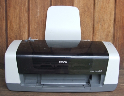
Inkjet printing is a type of computer printing that recreates a digital image by propelling droplets of ink onto paper and plastic substrates. Inkjet printers were the most commonly used type of printer in 2008, and range from small inexpensive consumer models to expensive professional machines. By 2019, laser printers outsold inkjet printers by nearly a 2:1 ratio, 9.6% vs 5.1% of all computer peripherals. The concept of inkjet printing originated in the 20th century, and the technology was first extensively developed in the early 1950s. While working at Canon in Japan, Ichiro Endo suggested the idea for a "Bubble jet" printer, while around the same time Jon Vaught at HP was developing a similar idea. In the late 1970s, inkjet printers that could reproduce digital images generated by computers were developed, mainly by Epson, Hewlett-Packard (HP) and Canon. In the worldwide consumer market, four manufacturers account for the majority of inkjet printer sales: Canon, HP, Eps ... [...More Info...] [...Related Items...] OR: [Wikipedia] [Google] [Baidu] |
Thin-film
A thin film is a layer of material ranging from fractions of a nanometer (monolayer) to several micrometers in thickness. The controlled synthesis of materials as thin films (a process referred to as deposition) is a fundamental step in many applications. A familiar example is the household mirror, which typically has a thin metal coating on the back of a sheet of glass to form a reflective interface. The process of silvering was once commonly used to produce mirrors, while more recently the metal layer is deposited using techniques such as sputtering. Advances in thin film deposition techniques during the 20th century have enabled a wide range of technological breakthroughs in areas such as magnetic recording media, electronic semiconductor devices, integrated passive devices, LEDs, optical coatings (such as antireflective coatings), hard coatings on cutting tools, and for both energy generation (e.g. thin-film solar cells) and storage ( thin-film batteries). It is also being ... [...More Info...] [...Related Items...] OR: [Wikipedia] [Google] [Baidu] |
Accelerometer
An accelerometer is a tool that measures proper acceleration. Proper acceleration is the acceleration (the rate of change of velocity) of a body in its own instantaneous rest frame; this is different from coordinate acceleration, which is acceleration in a fixed coordinate system. For example, an accelerometer at rest on the surface of the Earth will measure an acceleration due to Earth's gravity, straight upwards (by definition) of g ≈ 9.81 m/s2. By contrast, accelerometers in free fall (falling toward the center of the Earth at a rate of about 9.81 m/s2) will measure zero. Accelerometers have many uses in industry and science. Highly sensitive accelerometers are used in inertial navigation systems for aircraft and missiles. Vibration in rotating machines is monitored by accelerometers. They are used in tablet computers and digital cameras so that images on screens are always displayed upright. In unmanned aerial vehicles, accelerometers help to stabilise flight. ... [...More Info...] [...Related Items...] OR: [Wikipedia] [Google] [Baidu] |
Air Bag
An airbag is a vehicle occupant-restraint system using a bag designed to inflate extremely quickly, then quickly deflate during a Traffic collision, collision. It consists of the airbag cushion, a flexible fabric bag, an inflation module, and an impact sensor. The purpose of the airbag is to provide a vehicle occupant with soft cushioning and restraint during a collision. It can reduce injuries between the flailing occupant and the interior of the vehicle. The airbag provides an energy-absorbing surface between the vehicle's occupants and a steering wheel, instrument panel, Pillar (car), body pillar, headliner, and windshield. Modern vehicles may contain up to 10 airbag modules in various configurations, including: driver, passenger, side-curtain, seat-mounted, door-mounted, B and C-pillar mounted side-impact, knee bolster, inflatable seat belt, and pedestrian airbag modules. During a crash, the vehicle's crash sensors provide crucial information to the airbag electronic contro ... [...More Info...] [...Related Items...] OR: [Wikipedia] [Google] [Baidu] |
MEMs
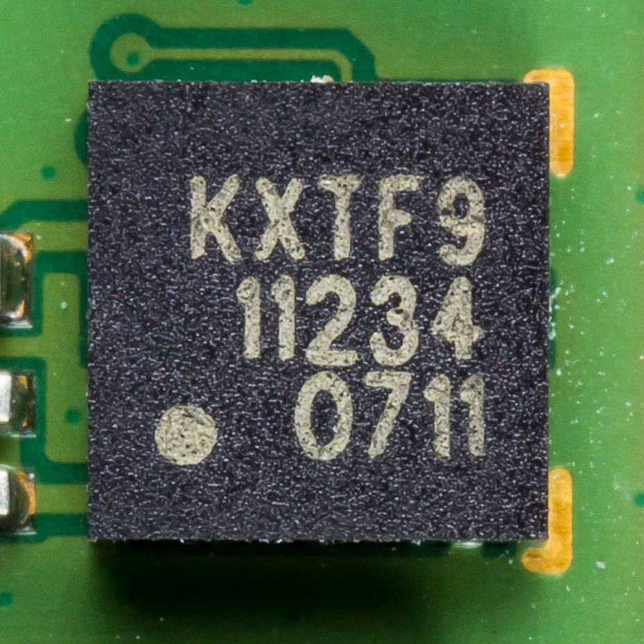
Microelectromechanical systems (MEMS), also written as micro-electro-mechanical systems (or microelectronic and microelectromechanical systems) and the related micromechatronics and microsystems constitute the technology of microscopic devices, particularly those with moving parts. They merge at the nanoscale into nanoelectromechanical systems (NEMS) and nanotechnology. MEMS are also referred to as micromachines in Japan and microsystem technology (MST) in Europe. MEMS are made up of components between 1 and 100 micrometers in size (i.e., 0.001 to 0.1 mm), and MEMS devices generally range in size from 20 micrometres to a millimetre (i.e., 0.02 to 1.0 mm), although components arranged in arrays (e.g., digital micromirror devices) can be more than 1000 mm2. They usually consist of a central unit that processes data (an integrated circuit chip such as microprocessor) and several components that interact with the surroundings (such as microsensors). Because of the la ... [...More Info...] [...Related Items...] OR: [Wikipedia] [Google] [Baidu] |


_250_nm_by_250_nm_image_of_one-atom-thick_silver_islands_grown_on_palladium_(111)_surface.png)


