|
MEMS
MEMS (micro-electromechanical systems) is the technology of microscopic devices incorporating both electronic and moving parts. MEMS are made up of components between 1 and 100 micrometres in size (i.e., 0.001 to 0.1 mm), and MEMS devices generally range in size from 20 micrometres to a millimetre (i.e., 0.02 to 1.0 mm), although components arranged in arrays (e.g., digital micromirror devices) can be more than 1000 mm2. They usually consist of a central unit that processes data (an integrated circuit chip such as microprocessor) and several components that interact with the surroundings (such as microsensors). Because of the large surface area to volume ratio of MEMS, forces produced by ambient electromagnetism (e.g., electrostatic charges and magnetic moments), and fluid dynamics (e.g., surface tension and viscosity) are more important design considerations than with larger scale mechanical devices. MEMS technology is distinguished from molecular nanotechnolo ... [...More Info...] [...Related Items...] OR: [Wikipedia] [Google] [Baidu] |
Nanoelectromechanical Systems
Nanoelectromechanical systems (NEMS) are a class of devices integrating electrical and mechanical functionality on the nanoscale. NEMS form the next logical miniaturization step from so-called microelectromechanical systems, or MEMS devices. NEMS typically integrate transistor-like nanoelectronics with mechanical actuators, pumps, or motors, and may thereby form physical, biological, and chemical sensors. The name derives from typical device dimensions in the nanometer range, leading to low mass, high mechanical resonance frequencies, potentially large quantum mechanical effects such as zero point motion, and a high surface-to-volume ratio useful for surface-based sensing mechanisms. Applications include accelerometers and sensors to detect chemical substances in the air. History Background As noted by Richard Feynman in his famous talk in 1959, " There's Plenty of Room at the Bottom," there are many potential applications of machines at smaller and smaller sizes; by buildi ... [...More Info...] [...Related Items...] OR: [Wikipedia] [Google] [Baidu] |
Integrated Circuit
An integrated circuit (IC), also known as a microchip or simply chip, is a set of electronic circuits, consisting of various electronic components (such as transistors, resistors, and capacitors) and their interconnections. These components are etched onto a small, flat piece ("chip") of semiconductor material, usually silicon. Integrated circuits are used in a wide range of electronic devices, including computers, smartphones, and televisions, to perform various functions such as processing and storing information. They have greatly impacted the field of electronics by enabling device miniaturization and enhanced functionality. Integrated circuits are orders of magnitude smaller, faster, and less expensive than those constructed of discrete components, allowing a large transistor count. The IC's mass production capability, reliability, and building-block approach to integrated circuit design have ensured the rapid adoption of standardized ICs in place of designs using discre ... [...More Info...] [...Related Items...] OR: [Wikipedia] [Google] [Baidu] |
Semiconductor Device Fabrication
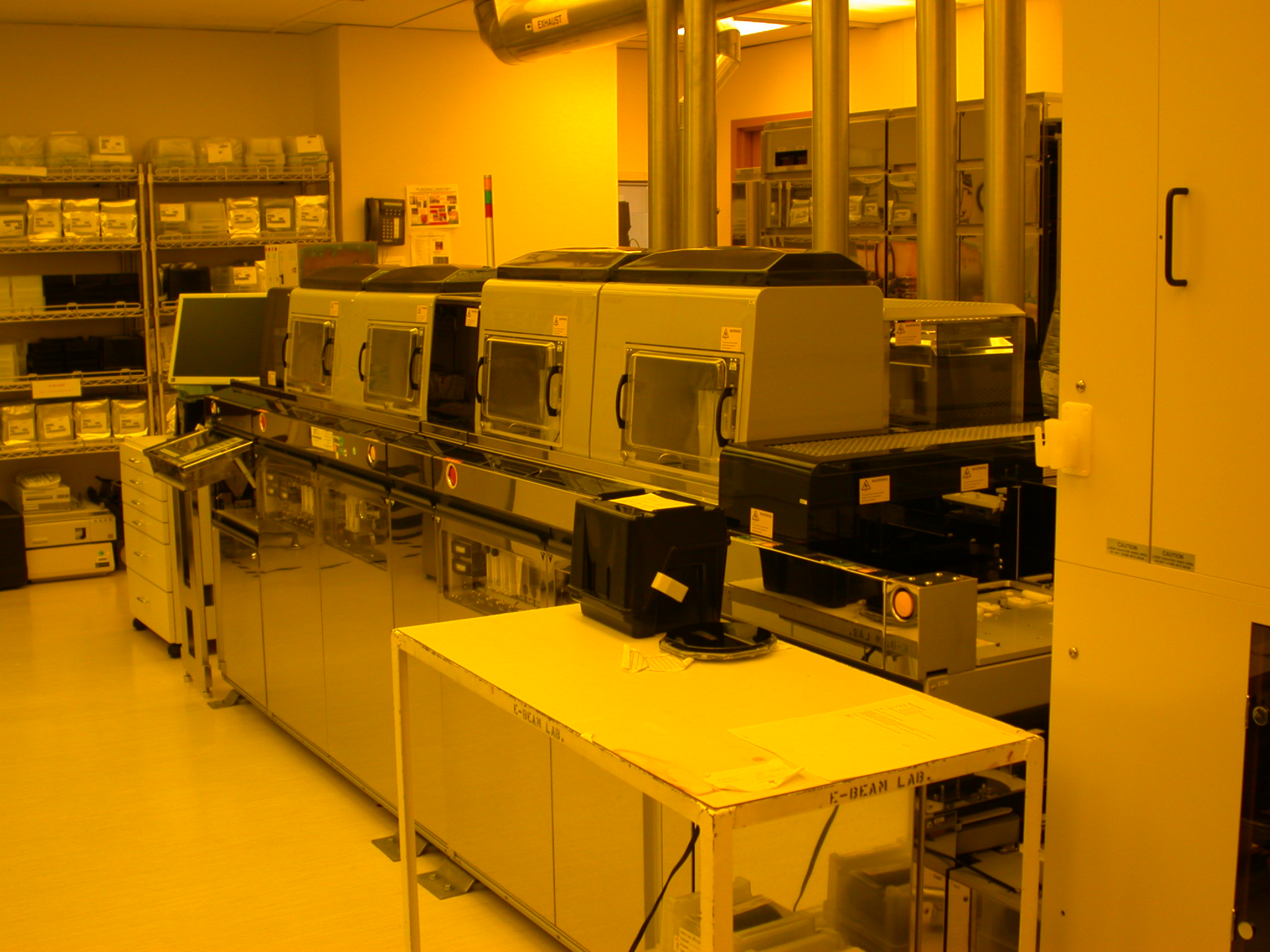
Semiconductor device fabrication is the process used to manufacture semiconductor devices, typically integrated circuits (ICs) such as microprocessors, microcontrollers, and memories (such as Random-access memory, RAM and flash memory). It is a multiple-step Photolithography, photolithographic and physico-chemical process (with steps such as thermal oxidation, thin-film deposition, ion-implantation, etching) during which electronic circuits are gradually created on a wafer (electronics), wafer, typically made of pure single-crystal semiconducting material. Silicon is almost always used, but various compound semiconductors are used for specialized applications. This article focuses on the manufacture of integrated circuits, however steps such as etching and photolithography can be used to manufacture other devices such as LCD and OLED displays. The fabrication process is performed in highly specialized semiconductor fabrication plants, also called foundries or "fabs", with the cen ... [...More Info...] [...Related Items...] OR: [Wikipedia] [Google] [Baidu] |
Microsensor
A sensor is often defined as a device that receives and responds to a signal or stimulus. The stimulus is the quantity, property, or condition that is sensed and converted into electrical signal. In the broadest definition, a sensor is a device, module, machine, or subsystem that detects events or changes in its environment and sends the information to other electronics, frequently a computer processor. Sensors are used in everyday objects such as touch-sensitive elevator buttons (tactile sensor) and lamps which dim or brighten by touching the base, and in innumerable applications of which most people are never aware. With advances in micromachinery and easy-to-use microcontroller platforms, the uses of sensors have expanded beyond the traditional fields of temperature, pressure and flow measurement, for example into Attitude and heading reference system, MARG sensors. Analog sensors such as potentiometers and force-sensing resistors are still widely used. Their applications ... [...More Info...] [...Related Items...] OR: [Wikipedia] [Google] [Baidu] |
Digital Micromirror Device
The digital micromirror device, or DMD, is the microoptoelectromechanical system (MOEMS) that is the core of the trademarked Digital Light Processing (DLP) projection technology from Texas Instruments (TI). The device is used in digital projectors and consists of an array of millions of microscopic mirrors which can be individually tilted many thousand times per second, thereby creating the pixels of the projected images. History The technology goes back to 1973 with Harvey C. Nathanson's (inventor of MEMS c. 1965) use of millions of microscopically small moving mirrors to create a video display of the type now found in digital projectors. The project at Texas Instrument's began as the deformable mirror device in 1977 using micromechanical analog light modulators. The DMD was invented by solid-state physicist and TI Fellow Emeritus Dr. Larry Hornbeck in 1987. The first analog DMD product was the TI DMD2000 airline ticket printer that went to market in 1990 and used a DM ... [...More Info...] [...Related Items...] OR: [Wikipedia] [Google] [Baidu] |
Microscopy
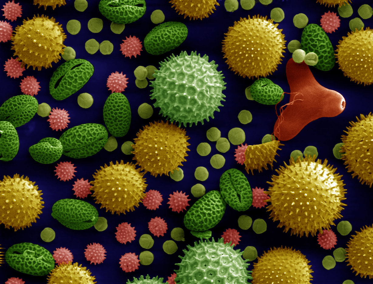
Microscopy is the technical field of using microscopes to view subjects too small to be seen with the naked eye (objects that are not within the resolution range of the normal eye). There are three well-known branches of microscopy: optical microscope, optical, electron microscope, electron, and scanning probe microscopy, along with the emerging field of X-ray microscopy. Optical microscopy and electron microscopy involve the diffraction, reflection (physics), reflection, or refraction of electromagnetic radiation/electron beams interacting with the Laboratory specimen, specimen, and the collection of the scattered radiation or another signal in order to create an image. This process may be carried out by wide-field irradiation of the sample (for example standard light microscopy and transmission electron microscope, transmission electron microscopy) or by scanning a fine beam over the sample (for example confocal laser scanning microscopy and scanning electron microscopy). Scan ... [...More Info...] [...Related Items...] OR: [Wikipedia] [Google] [Baidu] |
Nanotechnology
Nanotechnology is the manipulation of matter with at least one dimension sized from 1 to 100 nanometers (nm). At this scale, commonly known as the nanoscale, surface area and quantum mechanical effects become important in describing properties of matter. This definition of nanotechnology includes all types of research and technologies that deal with these special properties. It is common to see the plural form "nanotechnologies" as well as "nanoscale technologies" to refer to research and applications whose common trait is scale. An earlier understanding of nanotechnology referred to the particular technological goal of precisely manipulating atoms and molecules for fabricating macroscale products, now referred to as molecular nanotechnology. Nanotechnology defined by scale includes fields of science such as surface science, organic chemistry, molecular biology, semiconductor physics, energy storage, engineering, microfabrication, and molecular engineering. The associated rese ... [...More Info...] [...Related Items...] OR: [Wikipedia] [Google] [Baidu] |
Etching (microfabrication)
Etching is used in microfabrication to chemically remove layers from the surface of a wafer (electronics), wafer during manufacturing. Etching is a critically important process module in fabrication, and every wafer undergoes many etching steps before it is complete. For many etch steps, part of the wafer is protected from the etchant by a "masking" material which resists etching. In some cases, the masking material is a photoresist which has been patterned using photolithography. Other situations require a more durable mask, such as silicon nitride. Etching media and technology The two fundamental types of etchants are liquid-phase ("wet") and plasma (physics), plasma-phase ("dry"). Each of these exists in several varieties. Wet etching The first etching processes used liquid-phase ("wet") etchants. This process is now largely outdated but was used up until the late 1980s when it was superseded by dry plasma etching. The wafer can be immersed in a bath of etchant, wh ... [...More Info...] [...Related Items...] OR: [Wikipedia] [Google] [Baidu] |
Molecular Nanotechnology
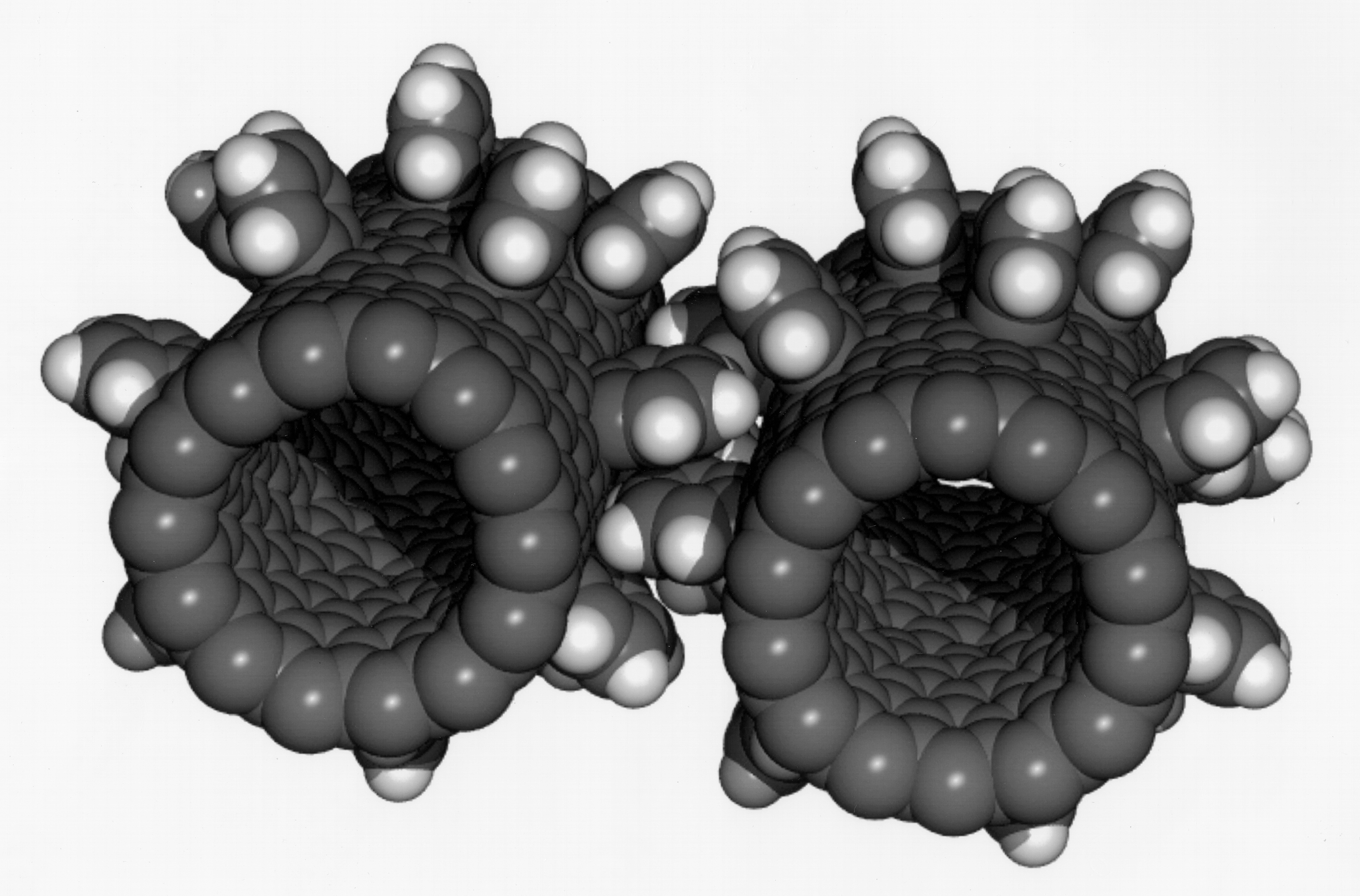
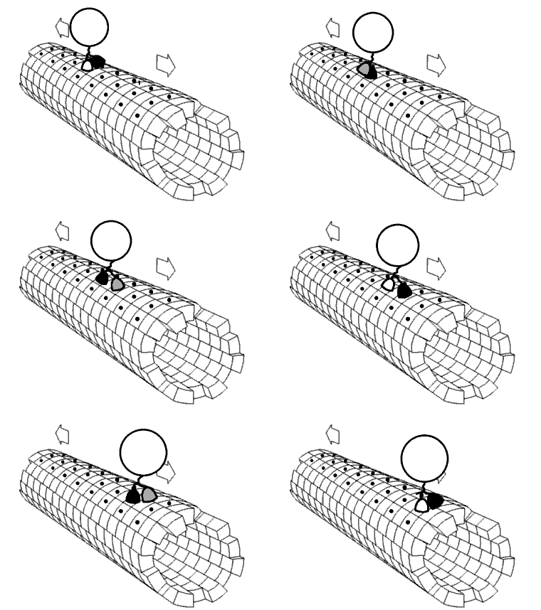
Molecular nanotechnology (MNT) is a technology based on the ability to build structures to complex, atomic specifications by means of mechanosynthesis. This is distinct from nanoscale materials. Based on Richard Feynman's vision of miniature factories using nanomachines to build complex products ( including additional nanomachines), this advanced form of nanotechnology (or ''molecular manufacturing'') would make use of positionally-controlled mechanosynthesis guided by molecular machine systems. MNT would involve combining physical principles demonstrated by biophysics, chemistry, other nanotechnologies, and the molecular machinery of life, with the systems engineering principles found in modern macroscale factories. Introduction While conventional chemistry uses inexact processes obtaining inexact results, and biology exploits inexact processes to obtain definitive results, molecular nanotechnology would employ original definitive processes to obtain definitive resul ... [...More Info...] [...Related Items...] OR: [Wikipedia] [Google] [Baidu] |
Potassium Hydroxide
Potassium hydroxide is an inorganic compound with the formula K OH, and is commonly called caustic potash. Along with sodium hydroxide (NaOH), KOH is a prototypical strong base. It has many industrial and niche applications, most of which utilize its caustic nature and its reactivity toward acids. An estimated 700,000 to 800,000 tonnes were produced in 2005. KOH is noteworthy as the precursor to most soft and liquid soaps, as well as numerous potassium-containing chemicals. It is a white solid that is dangerously corrosive. Properties and structure KOH exhibits high thermal stability. Because of this high stability and relatively low melting point, it is often melt-cast as pellets or rods, forms that have low surface area and convenient handling properties. These pellets become tacky in air because KOH is hygroscopic. Most commercial samples are ca. 90% pure, the remainder being water and carbonates. Its dissolution in water is strongly exothermic. Concentrated aqueous ... [...More Info...] [...Related Items...] OR: [Wikipedia] [Google] [Baidu] |
Scientific American
''Scientific American'', informally abbreviated ''SciAm'' or sometimes ''SA'', is an American popular science magazine. Many scientists, including Albert Einstein and Nikola Tesla, have contributed articles to it, with more than 150 Nobel Prize-winners being featured since its inception. In print since 1845, it is the oldest continuously published magazine in the United States. ''Scientific American'' is owned by Springer Nature, which is a subsidiary of Holtzbrinck Publishing Group. History ''Scientific American'' was founded by inventor and publisher Rufus Porter (painter), Rufus Porter in 1845 as a four-page weekly newspaper. The first issue of the large-format New York City newspaper was released on August 28, 1845. Throughout its early years, much emphasis was placed on reports of what was going on at the United States Patent and Trademark Office, U.S. Patent Office. It also reported on a broad range of inventions including perpetual motion machines, an 1860 devi ... [...More Info...] [...Related Items...] OR: [Wikipedia] [Google] [Baidu] |


