|
Ion-beam Sculpting
Ion-Beam sculpting is a two-step process to make solid-state nanopores. The term itself was coined by Golovchenko and co-workers at Harvard in the paper "Ion-beam sculpting at nanometer length scales." In the process, solid-state nanopores are formed by lateral mass transport about the surface of the substrate, not simply by sputtering, which is the removal of material from the surface. Basis The first step in ion sculpting is to make either a through hole or a blind hole, most commonly using a focused ion beam (FIB). The holes are commonly ~100 nm, but can be made much smaller. This step may or may not be done at room temperature, with a low temperature of -120 C. Next, there are three common techniques to now 'sculpt' the hole: broad area ion exposure, TEM exposure, and FIB exposure. Holes can be closed completely, but also they can be left open at a lower limit of 1 - 10 nm. Broad area ion exposure This technique uses a broad area argon ion source beam. If the ... [...More Info...] [...Related Items...] OR: [Wikipedia] [Google] [Baidu] |
Nanopore
A nanopore is a pore of nanometer size. It may, for example, be created by a pore-forming protein or as a hole in synthetic materials such as silicon or graphene. When a nanopore is present in an electrically insulating membrane, it can be used as a single-molecule detector. It can be a biological protein channel in a high electrical resistance lipid bilayer, a pore in a solid-state membrane or a hybrid of these – a protein channel set in a synthetic membrane. The detection principle is based on monitoring the ionic current passing through the nanopore as a voltage is applied across the membrane. When the nanopore is of molecular dimensions, passage of molecules (e.g., DNA) cause interruptions of the "open" current level, leading to a "translocation event" signal. The passage of RNA or single-stranded DNA molecules through the membrane-embedded alpha-hemolysin channel (1.5 nm diameter), for example, causes a ~90% blockage of the current (measured at 1 M KCl solution). It m ... [...More Info...] [...Related Items...] OR: [Wikipedia] [Google] [Baidu] |
Ion Source
An ion source is a device that creates atomic and molecular ions. Ion sources are used to form ions for mass spectrometers, optical emission spectrometers, particle accelerators, ion implanters and ion engines. Electron ionization Electron ionization is widely used in mass spectrometry, particularly for organic molecules. The gas phase reaction producing electron ionization is :M + e^- -> M^ + 2e^- where M is the atom or molecule being ionized, e^- is the electron, and M^ is the resulting ion. The electrons may be created by an arc discharge between a cathode and an anode. An electron beam ion source (EBIS) is used in atomic physics to produce highly charged ions by bombarding atoms with a powerful electron beam. Its principle of operation is shared by the electron beam ion trap. Electron capture ionization Electron capture ionization (ECI) is the ionization of a gas phase atom or molecule by attachment of an electron to create an ion of the form A−•. The reaction ... [...More Info...] [...Related Items...] OR: [Wikipedia] [Google] [Baidu] |
Ion Beam
An ion beam is a type of charged particle beam consisting of ions. Ion beams have many uses in electronics manufacturing (principally ion implantation) and other industries. A variety of ion beam sources exists, some derived from the mercury vapor thrusters developed by NASA in the 1960s. The most common ion beams are of singly-charged ions. Units Ion current density is typically measured in mA/cm^2, and ion energy in eV. The use of eV is convenient for converting between voltage and energy, especially when dealing with singly-charged ion beams, as well as converting between energy and temperature (1 eV = 11600 K). Broad-beam ion sources Most commercial applications use two popular types of ion source, gridded and gridless, which differ in current and power characteristics and the ability to control ion trajectories. In both cases electrons are needed to generate an ion beam. The most common electron emitters are hot filament and hollow cathode. Gridded ion source In a ... [...More Info...] [...Related Items...] OR: [Wikipedia] [Google] [Baidu] |
Focused Ion Beam
Focused ion beam, also known as FIB, is a technique used particularly in the semiconductor industry, materials science and increasingly in the biological field for site-specific analysis, deposition, and ablation of materials. A FIB setup is a scientific instrument that resembles a scanning electron microscope (SEM). However, while the SEM uses a focused beam of electrons to image the sample in the chamber, a FIB setup uses a focused beam of ions instead. FIB can also be incorporated in a system with both electron and ion beam columns, allowing the same feature to be investigated using either of the beams. FIB should not be confused with using a beam of focused ions for direct write lithography (such as in proton beam writing). These are generally quite different systems where the material is modified by other mechanisms. Ion beam source Most widespread instruments are using liquid metal ion sources (LMIS), especially gallium ion sources. Ion sources based on elemental gold an ... [...More Info...] [...Related Items...] OR: [Wikipedia] [Google] [Baidu] |
1 E-7 M
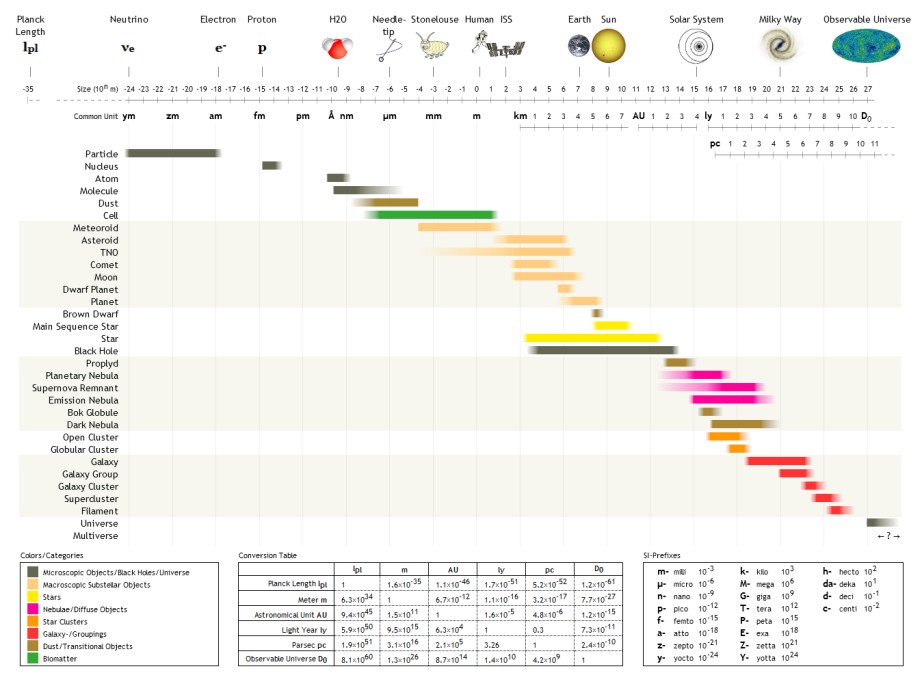
The following are examples of orders of magnitude for different lengths. __TOC__ Overview Detailed list To help compare different orders of magnitude, the following list describes various lengths between 1.6 \times 10^ metres and 10^metres. Subatomic scale Atomic to cellular scale Cellular to human scale Human to astronomical scale Astronomical scale Less than 1 zeptometre The ' ( SI symbol: ') is a unit of length in the metric system equal to . To help compare different orders of magnitude, this section lists lengths shorter than 10−21 m (1 zm). *1.6 × 10⁻⁵ quectometres (1.6 × 10⁻³⁵ metres) – the Planck length (Measures of distance shorter than this do not make physical sense, according to current theories of physics.) *1 qm – 1 quectometre, the smallest named subdivision of the metre in the SI base unit of length, one nonillionth of a metre *1 rm – 1 rontometre, a subdivision of the metre in the SI base unit of length, one octilliont ... [...More Info...] [...Related Items...] OR: [Wikipedia] [Google] [Baidu] |
Transmission Electron Microscope
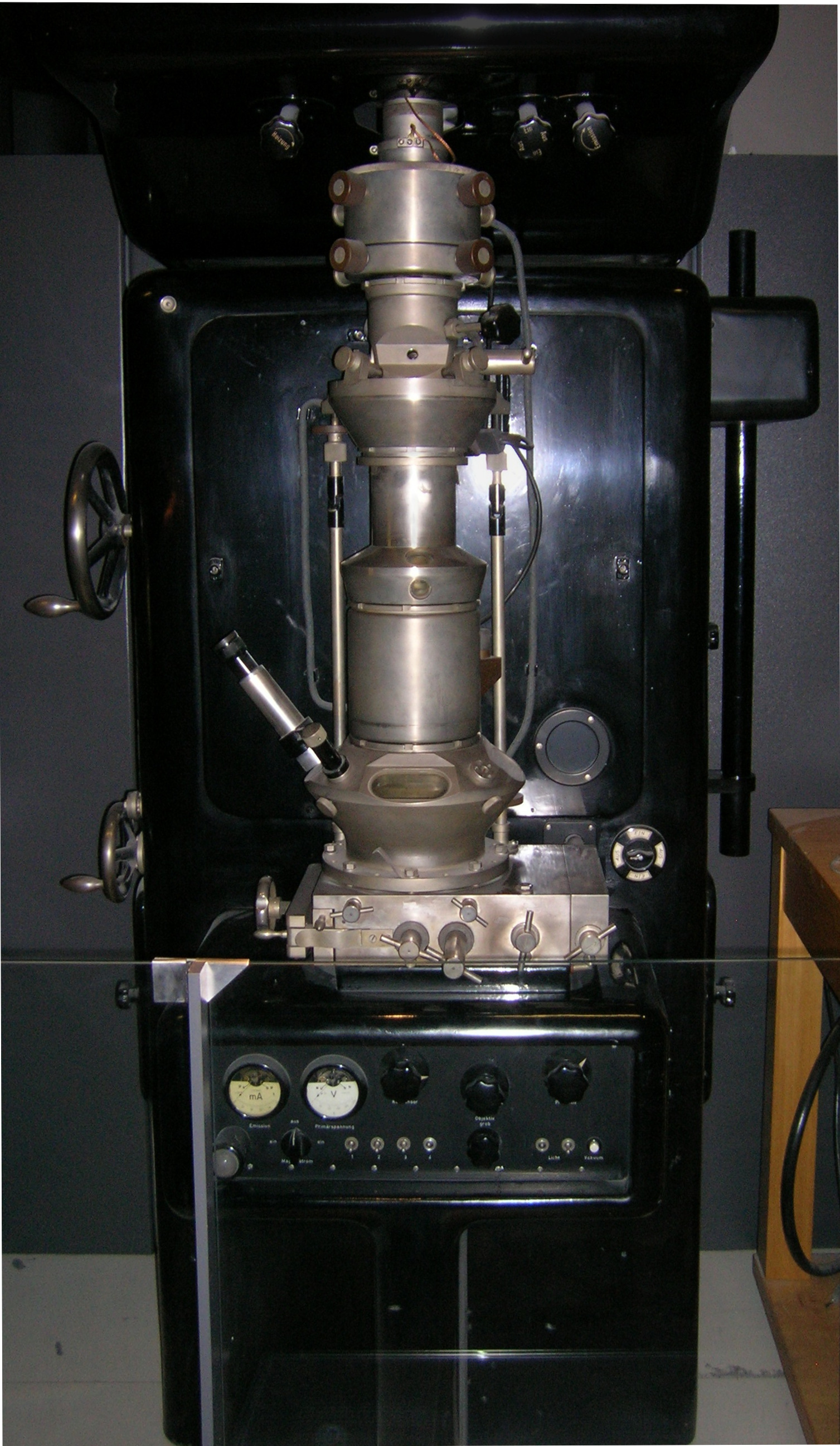
Transmission electron microscopy (TEM) is a microscopy technique in which a beam of electrons is transmitted through a specimen to form an image. The specimen is most often an ultrathin section less than 100 nm thick or a suspension on a grid. An image is formed from the interaction of the electrons with the sample as the beam is transmitted through the specimen. The image is then magnified and focused onto an imaging device, such as a fluorescent screen, a layer of photographic film, or a sensor such as a scintillator attached to a charge-coupled device. Transmission electron microscopes are capable of imaging at a significantly higher resolution than light microscopes, owing to the smaller de Broglie wavelength of electrons. This enables the instrument to capture fine detail—even as small as a single column of atoms, which is thousands of times smaller than a resolvable object seen in a light microscope. Transmission electron microscopy is a major analytical method in ... [...More Info...] [...Related Items...] OR: [Wikipedia] [Google] [Baidu] |
Noble Gas
The noble gases (historically also the inert gases; sometimes referred to as aerogens) make up a class of chemical elements with similar properties; under standard conditions, they are all odorless, colorless, monatomic gases with very low chemical reactivity. The six naturally occurring noble gases are helium (He), neon (Ne), argon (Ar), krypton (Kr), xenon (Xe), and the radioactive radon (Rn). Oganesson (Og) is a synthetically produced highly radioactive element. Although IUPAC has used the term "noble gas" interchangeably with "group 18" and thus included oganesson, it may not be significantly chemically noble and is predicted to break the trend and be reactive due to relativistic effects. Because of the extremely short 0.7 ms half-life of its only known isotope, its chemistry has not yet been investigated. For the first six periods of the periodic table, the noble gases are exactly the members of group 18. Noble gases are typically highly unreactive except when u ... [...More Info...] [...Related Items...] OR: [Wikipedia] [Google] [Baidu] |
Silicon Dioxide
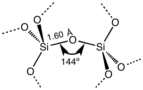
Silicon dioxide, also known as silica, is an oxide of silicon with the chemical formula , most commonly found in nature as quartz and in various living organisms. In many parts of the world, silica is the major constituent of sand. Silica is one of the most complex and most abundant families of materials, existing as a compound of several minerals and as a synthetic product. Notable examples include fused quartz, fumed silica, silica gel, opal and aerogels. It is used in structural materials, microelectronics (as an electrical insulator), and as components in the food and pharmaceutical industries. Structure In the majority of silicates, the silicon atom shows tetrahedral coordination, with four oxygen atoms surrounding a central Si atomsee 3-D Unit Cell. Thus, SiO2 forms 3-dimensional network solids in which each silicon atom is covalently bonded in a tetrahedral manner to 4 oxygen atoms. In contrast, CO2 is a linear molecule. The starkly different structures of the dioxid ... [...More Info...] [...Related Items...] OR: [Wikipedia] [Google] [Baidu] |
Silicon Nitride
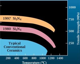
Silicon nitride is a chemical compound of the elements silicon and nitrogen. is the most thermodynamically stable and commercially important of the silicon nitrides, and the term "silicon nitride" commonly refers to this specific composition. It is a white, high-melting-point solid that is relatively chemically inert, being attacked by dilute HF and hot . It is very hard (8.5 on the mohs scale). It has a high thermal stability with strong optical nonlinearities for all-optical applications. Production Silicon nitride is prepared by heating powdered silicon between 1300 °C and 1400 °C in a nitrogen atmosphere: :3 Si + 2 → The silicon sample weight increases progressively due to the chemical combination of silicon and nitrogen. Without an iron catalyst, the reaction is complete after several hours (~7), when no further weight increase due to nitrogen absorption (per gram of silicon) is detected. In addition to , several other silicon nitride phases (with chemical ... [...More Info...] [...Related Items...] OR: [Wikipedia] [Google] [Baidu] |
Wafer (electronics)
In electronics, a wafer (also called a slice or substrate) is a thin slice of semiconductor, such as a crystalline silicon Crystalline silicon or (c-Si) Is the crystalline forms of silicon, either polycrystalline silicon (poly-Si, consisting of small crystals), or monocrystalline silicon (mono-Si, a continuous crystal). Crystalline silicon is the dominant semiconduc ... (c-Si), used for the fabrication of integrated circuits and, in photovoltaics, to manufacture solar cells. The wafer serves as the substrate (materials science), substrate for microelectronic devices built in and upon the wafer. It undergoes many microfabrication processes, such as doping (semiconductor), doping, ion implantation, Etching (microfabrication), etching, thin-film deposition of various materials, and Photolithography, photolithographic patterning. Finally, the individual microcircuits are separated by wafer dicing and Integrated circuit packaging, packaged as an integrated circuit. History I ... [...More Info...] [...Related Items...] OR: [Wikipedia] [Google] [Baidu] |
Blind Hole
A hole is an opening in or through a particular medium, usually a solid body. Holes occur through natural and artificial processes, and may be useful for various purposes, or may represent a problem needing to be addressed in many fields of engineering. Depending on the material and the placement, a hole may be an indentation in a surface (such as a hole in the ground), or may pass completely through that surface (such as a hole created by a hole puncher in a piece of paper). Types Holes can occur for a number of reasons, including natural processes and intentional actions by humans or animals. Holes in the ground that are made intentionally, such as holes made while searching for food, for replanting trees, or postholes made for securing an object, are usually made through the process of digging. Unintentional holes in an object are often a sign of damage. Potholes and sinkholes can damage human settlements. Holes can occur in a wide variety of materials, and at a wide rang ... [...More Info...] [...Related Items...] OR: [Wikipedia] [Google] [Baidu] |
Argon
Argon is a chemical element with the symbol Ar and atomic number 18. It is in group 18 of the periodic table and is a noble gas. Argon is the third-most abundant gas in Earth's atmosphere, at 0.934% (9340 ppmv). It is more than twice as abundant as water vapor (which averages about 4000 ppmv, but varies greatly), 23 times as abundant as carbon dioxide (400 ppmv), and more than 500 times as abundant as neon (18 ppmv). Argon is the most abundant noble gas in Earth's crust, comprising 0.00015% of the crust. Nearly all of the argon in Earth's atmosphere is radiogenic argon-40, derived from the decay of potassium-40 in Earth's crust. In the universe, argon-36 is by far the most common argon isotope, as it is the most easily produced by stellar nucleosynthesis in supernovas. The name "argon" is derived from the Greek word , neuter singular form of meaning 'lazy' or 'inactive', as a reference to the fact that the element undergoes almost no chemical reactions. The complete octe ... [...More Info...] [...Related Items...] OR: [Wikipedia] [Google] [Baidu] |
.jpg)


