|
Failure Analysis
Failure analysis is the process of collecting and analyzing data to determine the cause of a failure, often with the goal of determining corrective actions or liability. According to Bloch and Geitner, ”machinery failures reveal a reaction chain of cause and effect… usually a deficiency commonly referred to as the symptom…”. Failure analysis can save money, lives, and resources if done correctly and acted upon. It is an important discipline in many branches of manufacturing industry, such as the electronics industry, where it is a vital tool used in the development of new products and for the improvement of existing products. The failure analysis process relies on collecting failed components for subsequent examination of the cause or causes of failure using a wide array of methods, especially microscopy and spectroscopy. Nondestructive testing (NDT) methods (such as industrial computed tomography scanning) are valuable because the failed products are unaffected by analysis ... [...More Info...] [...Related Items...] OR: [Wikipedia] [Google] [Baidu] |
Failure
Failure is the social concept of not meeting a desirable or intended objective, and is usually viewed as the opposite of success. The criteria for failure depends on context, and may be relative to a particular observer or belief system. One person might consider a failure what another person considers a success, particularly in cases of direct competition or a zero-sum game. Similarly, the degree of success or failure in a situation may be differently viewed by distinct observers or participants, such that a situation that one considers to be a failure, another might consider to be a success, a qualified success or a neutral situation. It may also be difficult or impossible to ascertain whether a situation meets criteria for failure or success due to ambiguous or ill-defined definition of those criteria. Finding useful and effective criteria or heuristics to judge the success or failure of a situation may itself be a significant task. Sociology Cultural historian Scot ... [...More Info...] [...Related Items...] OR: [Wikipedia] [Google] [Baidu] |
Scanning Acoustic Microscope
A scanning acoustic microscope (SAM) is a device which uses focused sound to investigate, measure, or image an object (a process called scanning acoustic tomography). It is commonly used in failure analysis and non-destructive evaluation. It also has applications in biological and medical research. The semiconductor industry has found the SAM useful in detecting voids, cracks, and delaminations within microelectronic packages. History The first scanning acoustic microscope (SAM), with a 50 MHz ultrasonic lens, was developed in 1974 by R. A. Lemons and C. F. Quate at the Microwave Laboratory of Stanford University. A few years later, in 1980, the first high-resolution (with a frequency up to 500 MHz) through-transmission SAM was built by R.Gr. Maev and his students at his Laboratory of Biophysical Introscopy of the Russian Academy of Sciences. First commercial SAM ELSAM, with a broad frequency range from 100 MHz up to 1.8 GHz, was built at the Ernst Leitz Gmb ... [...More Info...] [...Related Items...] OR: [Wikipedia] [Google] [Baidu] |
Deep-level Transient Spectroscopy
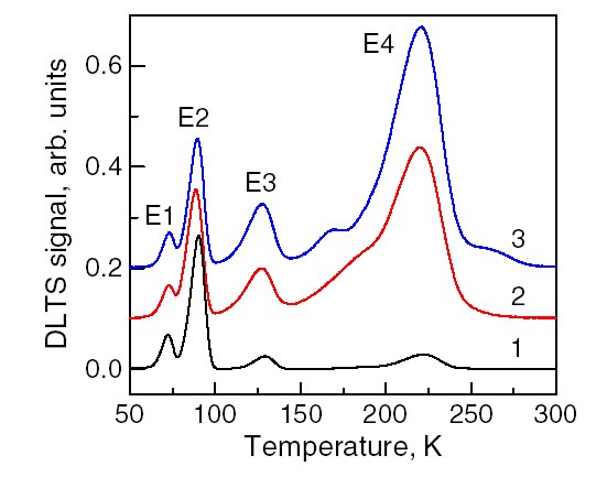
Deep-level transient spectroscopy (DLTS) is an experimental tool for studying electrically active defects (known as charge carrier traps) in semiconductors. DLTS establishes fundamental defect parameters and measures their concentration in the material. Some of the parameters are considered as defect "finger prints" used for their identifications and analysis. DLTS investigates defects present in a space charge (depletion region, depletion) region of a simple electronic device. The most commonly used are Schottky diodes or p-n junctions. In the measurement process the steady-state diode reverse polarization voltage is disturbed by a voltage Pulse (signal processing), pulse. This voltage pulse reduces the electric field in the space charge region and allows free Charge carrier, carriers from the semiconductor bulk to penetrate this region and recharge the defects causing their non-equilibrium charge state. After the pulse, when the voltage returns to its steady-state value, the defect ... [...More Info...] [...Related Items...] OR: [Wikipedia] [Google] [Baidu] |
Auger Electron Spectroscopy
A Hanford scientist uses an Auger electron spectrometer to determine the elemental composition of surfaces. Auger electron spectroscopy (AES; pronounced in French) is a common analytical technique used specifically in the study of surfaces and, more generally, in the area of materials science. It is a form of electron spectroscopy that relies on the Auger effect, based on the analysis of energetic electrons emitted from an excited atom after a series of internal relaxation events. The Auger effect was discovered independently by both Lise Meitner and Pierre Auger in the 1920s. Though the discovery was made by Meitner and initially reported in the journal ''Zeitschrift für Physik'' in 1922, Auger is credited with the discovery in most of the scientific community. Until the early 1950s Auger transitions were considered nuisance effects by spectroscopists, not containing much relevant material information, but studied so as to explain anomalies in X-ray spectroscopy data. Since 195 ... [...More Info...] [...Related Items...] OR: [Wikipedia] [Google] [Baidu] |
Transmission Line
In electrical engineering, a transmission line is a specialized cable or other structure designed to conduct electromagnetic waves in a contained manner. The term applies when the conductors are long enough that the wave nature of the transmission must be taken into account. This applies especially to radio-frequency engineering because the short wavelengths mean that wave phenomena arise over very short distances (this can be as short as millimetres depending on frequency). However, the Telegrapher's equations, theory of transmission lines was historically developed to explain phenomena on very long electrical telegraph, telegraph lines, especially submarine telegraph cables. Transmission lines are used for purposes such as connecting Transmitter, radio transmitters and Radio receiver, receivers with their antenna (radio), antennas (they are then called feed lines or feeders), distributing cable television signals, trunking, trunklines routing calls between telephone switchi ... [...More Info...] [...Related Items...] OR: [Wikipedia] [Google] [Baidu] |
Metallography
Metallography is the study of the physical structure and components of metals, by using microscopy. Ceramic and polymeric materials may also be prepared using metallographic techniques, hence the terms ceramography, plastography and, collectively, materialography. Preparing metallographic specimens The surface of a metallographic specimen is prepared by various methods of grinding (abrasive cutting), grinding, polishing, and Industrial etching, etching. After preparation, it is often analyzed using optical microscope, optical or electron microscopy. Using only metallographic techniques, a skilled technician can identify alloys and predict List of materials properties, material properties. Mechanical preparation is the most common preparation method. Successively finer abrasive particles are used to remove material from the sample surface until the desired surface quality is achieved. Many different machines are available for doing this Abrasive machining, grinding and po ... [...More Info...] [...Related Items...] OR: [Wikipedia] [Google] [Baidu] |
Plasma Etcher
Plasma etching is a form of plasma processing used to fabricate integrated circuits. It involves a high-speed stream of glow discharge (Plasma (physics), plasma) of an appropriate gas mixture being shot (in pulses) at a sample. The plasma source, known as etch species, can be either charged (ions) or neutral (atoms and radical (chemistry), radicals). During the process, the plasma generates volatile etch products at room temperature from the chemical reactions between the elements of the material etched and the reactive species generated by the plasma. Eventually the atoms of the shot element embed themselves at or just below the surface of the target, thus modifying the physical properties of the target. Mechanisms Plasma generation A plasma is a high energetic condition in which a lot of processes can occur. These processes happen because of electrons and atoms. To form the plasma electrons have to be accelerated to gain energy. Highly energetic electrons transfer the energy to ... [...More Info...] [...Related Items...] OR: [Wikipedia] [Google] [Baidu] |
USB Microscope
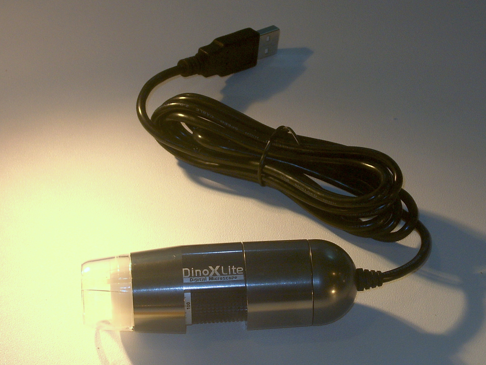
A USB microscope is a low-powered digital microscope which connects to a computer's USB port. Microscopes essentially the same as USB models are also available with other interfaces either in addition to or instead of USB, such as via WiFi. They are widely available at low cost for use at home or in commerce. Their cost varies in the range of tens to thousands of dollars. In essence, a USB microscope is a webcam with a high-powered macro lens, and generally uses reflected rather than transmitted light, using built-in LED light sources surrounding the lens. The camera is usually sensitive enough not to need additional illumination beyond normal ambient lighting. The camera attaches directly to the USB port of a computer without the need for an eyepiece, and the images are shown directly on the computer's display. They usually provide modest magnifications (about 1× to 200×) without the need to use eyepieces, at cost very much lower than conventional stereomicroscopes. [...More Info...] [...Related Items...] OR: [Wikipedia] [Google] [Baidu] |
Scanning SQUID Microscope
Scan, SCAN or Scanning may refer to: Science and technology Computing and electronics * Graham scan, an algorithm for finding the convex hull of a set of points in the plane * 3D scanning, of a real-world object or environment to collect three dimensional data * Counter-scanning, in physical micro and nanotopography measuring instruments like scanning probe microscope * Elevator algorithm or SCAN, a disk scheduling algorithm * Image scanning, an optical scan of images, printed text, handwriting or an object * Optical character recognition, optical recognition of printed text or printed sheet music * Port scanner, in computer networking * Prefix sum, an operation on lists that is also known as the scan operator * Raster scan, the rectangular pattern of image capture and reconstruction in television * Scan chain, a type of manufacturing test used with integrated circuits * Scan line, one line in a raster scanning pattern * Screen reading, on computers to quickly locate text elemen ... [...More Info...] [...Related Items...] OR: [Wikipedia] [Google] [Baidu] |
Infra-red
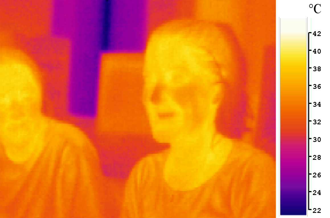
Infrared (IR; sometimes called infrared light) is electromagnetic radiation (EMR) with wavelengths longer than that of visible light but shorter than microwaves. The infrared spectral band begins with the waves that are just longer than those of red light (the longest waves in the visible spectrum), so IR is invisible to the human eye. IR is generally (according to ISO, CIE) understood to include wavelengths from around to . IR is commonly divided between longer-wavelength thermal IR, emitted from terrestrial sources, and shorter-wavelength IR or near-IR, part of the solar spectrum. Longer IR wavelengths (30–100 μm) are sometimes included as part of the terahertz radiation band. Almost all black-body radiation from objects near room temperature is in the IR band. As a form of EMR, IR carries energy and momentum, exerts radiation pressure, and has properties corresponding to both those of a wave and of a particle, the photon. It was long known that fires emit invisible ... [...More Info...] [...Related Items...] OR: [Wikipedia] [Google] [Baidu] |
X-ray Microscope
An X-ray microscope uses electromagnetic radiation in the X-ray band to produce magnified images of objects. Since X-rays penetrate most objects, there is no need to specially prepare them for X-ray microscopy observations. Unlike visible light, X-rays do not reflect or refract easily and are invisible to the human eye. Therefore, an X-ray microscope exposes film or uses a charge-coupled device (CCD) detector to detect X-rays that pass through the specimen. It is a contrast imaging technology using the difference in absorption of soft X-rays in the water window region (wavelengths: 2.34–4.4 nm, energies: 280–530 eV) by the carbon atom (main element composing the living cell) and the oxygen atom (an element of water). Microfocus X-ray also achieves high magnification by projection. A microfocus X-ray tube produces X-rays from an extremely small focal spot (5 μm down to 0.1 μm). The X-rays are in the more conventional X-ray range (20 to 300 keV) and ... [...More Info...] [...Related Items...] OR: [Wikipedia] [Google] [Baidu] |
Photon Emission Microscopy
A photon () is an elementary particle that is a quantum of the electromagnetic field, including electromagnetic radiation such as light and radio waves, and the force carrier for the electromagnetic force. Photons are massless particles that can move no faster than the speed of light measured in vacuum. The photon belongs to the class of boson particles. As with other elementary particles, photons are best explained by quantum mechanics and exhibit wave–particle duality, their behavior featuring properties of both waves and particles. The modern photon concept originated during the first two decades of the 20th century with the work of Albert Einstein, who built upon the research of Max Planck. While Planck was trying to explain how matter and electromagnetic radiation could be in thermal equilibrium with one another, he proposed that the energy stored within a material object should be regarded as composed of an integer number of discrete, equal-sized parts. To explain the pho ... [...More Info...] [...Related Items...] OR: [Wikipedia] [Google] [Baidu] |


