|
Bumpless Build-up Layer
Bumpless Build-up Layer or BBUL is a processor packaging technology developed by Intel. It is bumpless, because it does not use the usual tiny solder bumps to attach the silicon die to the processor package wires. It has build-up layers, because is grown or built up around the silicon die A die, in the context of integrated circuits, is a small block of semiconducting material on which a given functional circuit is fabricated. Typically, integrated circuits are produced in large batches on a single wafer of electronic-grade sili .... The usual way is to manufacture them separately and bond them together. It was presented in October 2001. It should have been a key component in the 8 GHz and 15 GHz processors that should have been in the market by 2005 and 2007 respectively. Also 20 GHz should have been possible before the year 2010. The BBUL is not needed yet because there is no longer the clock-frequency competition. Advantages * Thinner and lighter. * Higher pe ... [...More Info...] [...Related Items...] OR: [Wikipedia] [Google] [Baidu] |
Central Processing Unit
A central processing unit (CPU), also called a central processor, main processor or just processor, is the electronic circuitry that executes instructions comprising a computer program. The CPU performs basic arithmetic, logic, controlling, and input/output (I/O) operations specified by the instructions in the program. This contrasts with external components such as main memory and I/O circuitry, and specialized processors such as graphics processing units (GPUs). The form, design, and implementation of CPUs have changed over time, but their fundamental operation remains almost unchanged. Principal components of a CPU include the arithmetic–logic unit (ALU) that performs arithmetic and logic operations, processor registers that supply operands to the ALU and store the results of ALU operations, and a control unit that orchestrates the fetching (from memory), decoding and execution (of instructions) by directing the coordinated operations of the ALU, registers and oth ... [...More Info...] [...Related Items...] OR: [Wikipedia] [Google] [Baidu] |
Intel
Intel Corporation is an American multinational corporation and technology company headquartered in Santa Clara, California, Santa Clara, California. It is the world's largest semiconductor chip manufacturer by revenue, and is one of the developers of the x86 series of instruction sets, the instruction sets found in most personal computers (PCs). Delaware General Corporation Law, Incorporated in Delaware, Intel ranked No. 45 in the 2020 Fortune 500, ''Fortune'' 500 list of the largest United States corporations by total revenue for nearly a decade, from 2007 to 2016 fiscal years. Intel supplies microprocessors for List of computer system manufacturers, computer system manufacturers such as Acer Inc., Acer, Lenovo, HP Inc., HP, and Dell Technologies, Dell. Intel also manufactures motherboard chipsets, network interface controllers and integrated circuits, flash memory, Graphics processing unit, graphics chips, Embedded system, embedded processors and other devices related to com ... [...More Info...] [...Related Items...] OR: [Wikipedia] [Google] [Baidu] |
Solder
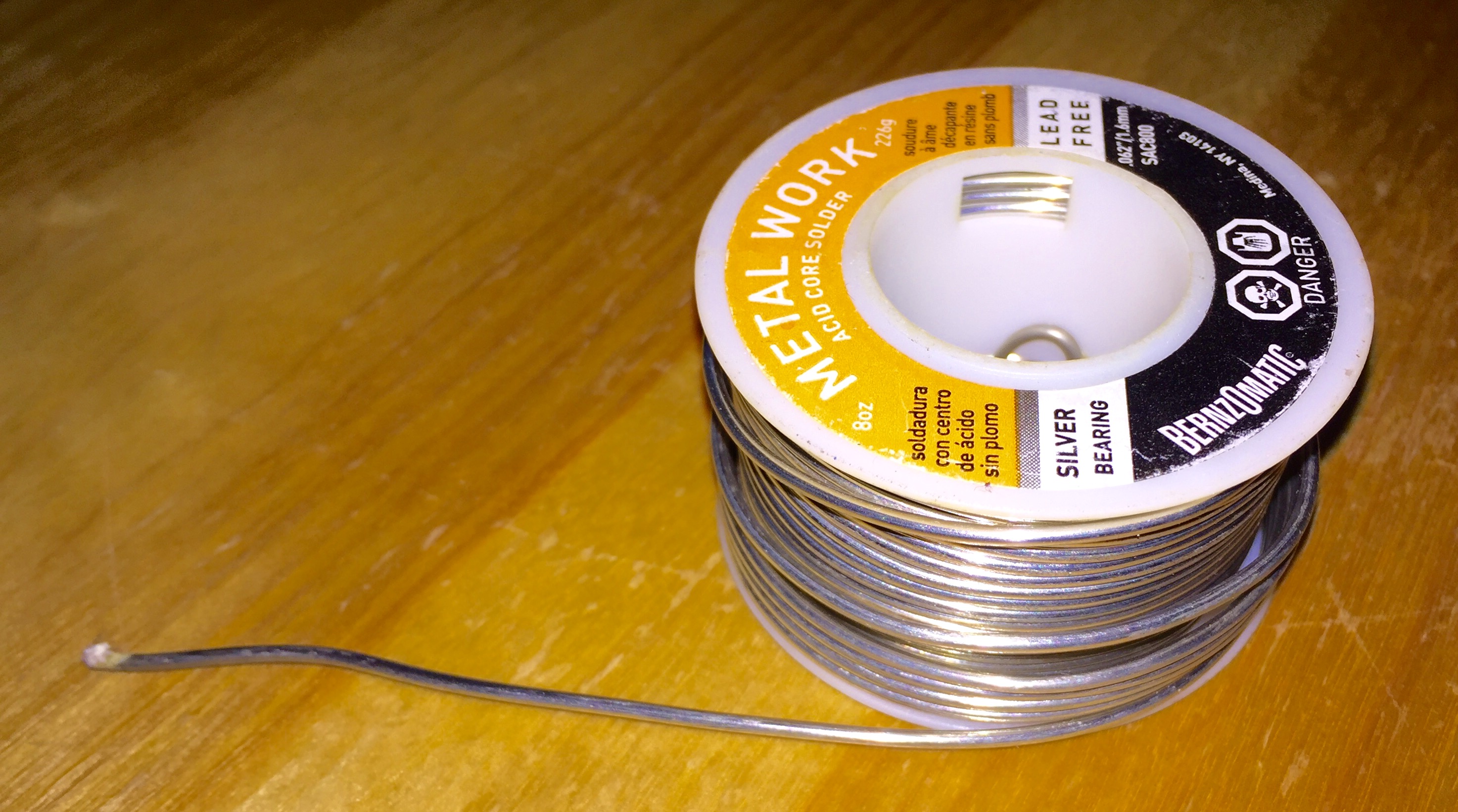
Solder (; NA: ) is a fusible metal alloy used to create a permanent bond between metal workpieces. Solder is melted in order to wet the parts of the joint, where it adheres to and connects the pieces after cooling. Metals or alloys suitable for use as solder should have a lower melting point than the pieces to be joined. The solder should also be resistant to oxidative and corrosive effects that would degrade the joint over time. Solder used in making electrical connections also needs to have favorable electrical characteristics. Soft solder typically has a melting point range of , and is commonly used in electronics, plumbing, and sheet metal work. Alloys that melt between are the most commonly used. Soldering performed using alloys with a melting point above is called "hard soldering", "silver soldering", or brazing. In specific proportions, some alloys are eutectic — that is, the alloy's melting point is the lowest possible for a mixture of those components, and ... [...More Info...] [...Related Items...] OR: [Wikipedia] [Google] [Baidu] |
Silicon Die
A die, in the context of integrated circuits, is a small block of semiconducting material on which a given functional circuit is fabricated. Typically, integrated circuits are produced in large batches on a single wafer of electronic-grade silicon (EGS) or other semiconductor (such as GaAs) through processes such as photolithography. The wafer is cut (diced) into many pieces, each containing one copy of the circuit. Each of these pieces is called a die. There are three commonly used plural forms: ''dice'', ''dies'' and ''die''. To simplify handling and integration onto a printed circuit board, most dies are packaged in various forms. Manufacturing process Most dies are composed of silicon and used for integrated circuits. The process begins with the production of monocrystalline silicon ingots. These ingots are then sliced into disks with a diameter of up to 300 mm. [...More Info...] [...Related Items...] OR: [Wikipedia] [Google] [Baidu] |
Flip Chip
Flip chip, also known as controlled collapse chip connection or its abbreviation, C4, is a method for interconnecting dies such as semiconductor devices, IC chips, integrated passive devices and microelectromechanical systems (MEMS), to external circuitry with solder bumps that have been deposited onto the chip pads. The technique was developed by General Electric's Light Military Electronics Department, Utica, New York. The solder bumps are deposited on the chip pads on the top side of the wafer during the final wafer processing step. In order to mount the chip to external circuitry (e.g., a circuit board or another chip or wafer), it is flipped over so that its top side faces down, and aligned so that its pads align with matching pads on the external circuit, and then the solder is reflowed to complete the interconnect. This is in contrast to wire bonding, in which the chip is mounted upright and fine wires are welded onto the chip pads and lead frame contacts to interconnect ... [...More Info...] [...Related Items...] OR: [Wikipedia] [Google] [Baidu] |


