Two-dimensional materials on:
[Wikipedia]
[Google]
[Amazon]
In materials science, the term single-layer materials or 2D materials refers to
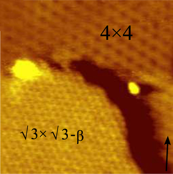 Silicene is a two-dimensional allotrope of silicon, with a hexagonal honeycomb structure similar to that of graphene. Its growth is scaffolded by a pervasive Si/Ag(111) surface alloy beneath the two-dimensional layer.
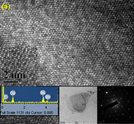
 Phosphorene is a 2-dimensional, crystalline allotrope of phosphorus. Its mono-atomic hexagonal structure makes it conceptually similar to graphene. However, phosphorene has substantially different electronic properties; in particular it possesses a nonzero band gap while displaying high electron mobility. This property potentially makes it a better semiconductor than graphene.
The synthesis of phosphorene mainly consists of micromechanical cleavage or liquid phase exfoliation methods. The former has a low yield while the latter produce free standing nanosheets in solvent and not on the solid support. The bottom-up approaches like chemical vapor deposition (CVD) are still blank because of its high reactivity. Therefore, in the current scenario, the most effective method for large area fabrication of thin films of phosphorene consists of wet assembly techniques like Langmuir-Blodgett involving the assembly followed by deposition of nanosheets on solid supports.
 Single and double atom layers of
 *
*
 The 2H phase of MoS2 ( Pearson symbol hP6; ''Strukturbericht'' designation C7) has space group P63/mmc. Each layer contains Mo surrounded by S in trigonal prismatic coordination. Conversely, the 1T phase (Pearson symbol hP3) has space group P-3m1, and octahedrally-coordinated Mo; with the 1T unit cell containing only one layer, the unit cell has a ''c'' parameter slightly less than half the length of that of the 2H unit cell (5.95 Å and 12.30 Å, respectively). The different crystal structures of the two phases result in differences in their electronic band structure as well. The d-orbitals of 2H-MoS2 are split into three bands: d''z''2, dx2-y2,xy, and dxz,yz. Of these, only the dz2 is filled; this combined with the splitting results in a semiconducting material with a bandgap of 1.9eV. 1T-MoS2, on the other hand, has partially filled d-orbitals which give it a metallic character.
Because the structure consists of in-plane covalent bonds and inter-layer
  While graphene has a hexagonal honeycomb lattice structure with alternating double-bonds emerging from its sp2-bonded carbons, graphane, still maintaining the hexagonal structure, is the fully hydrogenated version of graphene with every sp3-hybrized carbon bonded to a hydrogen (chemical formula of (CH)n). Furthermore, while graphene is planar due to its double-bonded nature, graphane is rugged, with the hexagons adopting different out-of-plane structural conformers like the chair or boat, to allow for the ideal 109.5° angles which reduce ring strain, in a direct analogy to the conformers of cyclohexane. Graphane was first theorized in 2003, was shown to be stable using first principles energy calculations in 2007, and was first experimentally synthesized in 2009. There are various experimental routes available for making graphane, including the top-down approaches of reduction of graphite in solution or hydrogenation of graphite using plasma/hydrogen gas as well as the bottom-up approach of chemical vapor deposition. Graphane is an insulator, with a predicted band gap of 3.5 eV; however, partially hydrogenated graphene is a semi-conductor, with the band gap being controlled by the degree of hydrogenation.
;Germanane
Germanane is a single-layer crystal composed of germanium with one hydrogen bonded in the z-direction for each atom. Germanane's structure is similar to graphane, Bulk germanium does not adopt this structure. Germanane is produced in a two-step route starting with
crystal
A crystal or crystalline solid is a solid material whose constituents (such as atoms, molecules, or ions) are arranged in a highly ordered microscopic structure, forming a crystal lattice that extends in all directions. In addition, macr ...
line solids consisting of a single layer of atoms. These materials are promising for some applications but remain the focus of research. Single-layer materials derived from single elements generally carry the -ene suffix in their names, e.g. graphene
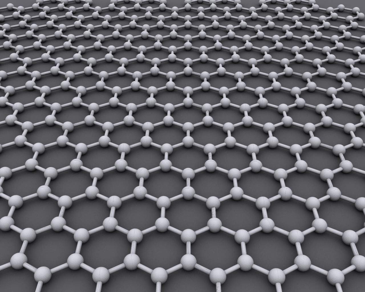
Graphene () is an allotrope of carbon consisting of a Single-layer materials, single layer of atoms arranged in a hexagonal lattice nanostructure.
. Single-layer materials that are compounds of two or more elements have -ane or -ide suffixes. 2D materials can generally be categorized as either 2D allotropes of various elements or as compounds (consisting of two or more covalently bonding elements).
It is predicted that there are hundreds of stable single-layer materials. The atomic structure and calculated basic properties of these and many other potentially synthesisable single-layer materials, can be found in computational databases. 2D materials can be produced using mainly two approaches: top-down exfoliation and bottom-up synthesis. The exfoliation methods include sonication, mechanical, hydrothermal, electrochemical, laser-assisted, and microwave-assisted exfoliation.
Single element materials
C: graphene and graphyne
;Graphene
Graphene
Graphene () is an allotrope of carbon consisting of a Single-layer materials, single layer of atoms arranged in a hexagonal lattice nanostructure.
is a crystal
A crystal or crystalline solid is a solid material whose constituents (such as atoms, molecules, or ions) are arranged in a highly ordered microscopic structure, forming a crystal lattice that extends in all directions. In addition, macr ...
line allotrope of carbon
Carbon () is a chemical element with the symbol C and atomic number 6. It is nonmetallic and tetravalent—its atom making four electrons available to form covalent chemical bonds. It belongs to group 14 of the periodic table. Carbon makes ...
in the form of a nearly transparent (to visible light) one atom thick sheet. It is hundreds of times stronger than most steels by weight. It has the highest known thermal and electrical conductivity, displaying current densities 1,000,000 times that of copper
Copper is a chemical element with the symbol Cu (from la, cuprum) and atomic number 29. It is a soft, malleable, and ductile metal with very high thermal and electrical conductivity. A freshly exposed surface of pure copper has a pinkish ...
. It was first produced in 2004.
Andre Geim and Konstantin Novoselov won the 2010 Nobel Prize in Physics
)
, image = Nobel Prize.png
, alt = A golden medallion with an embossed image of a bearded man facing left in profile. To the left of the man is the text "ALFR•" then "NOBEL", and on the right, the text (smaller) "NAT•" then " ...
"for groundbreaking experiments regarding the two-dimensional material graphene". They first produced it by lifting graphene flakes from bulk graphite with adhesive tape and then transferring them onto a silicon wafer.
;Graphyne
Graphyne is another 2-dimensional carbon allotrope whose structure is similar to graphene's. It can be seen as a lattice of benzene
Benzene is an organic chemical compound with the molecular formula C6H6. The benzene molecule is composed of six carbon atoms joined in a planar ring with one hydrogen atom attached to each. Because it contains only carbon and hydrogen ato ...
rings connected by acetylene bonds. Depending on the content of the acetylene groups, graphyne can be considered a mixed hybridization, spn, where 1 < n < 2, compared to graphene (pure sp2) and diamond
Diamond is a solid form of the element carbon with its atoms arranged in a crystal structure called diamond cubic. Another solid form of carbon known as graphite is the chemically stable form of carbon at room temperature and pressure, ...
(pure sp3).
First-principle calculations using phonon dispersion curves and ab-initio finite temperature, quantum mechanical molecular dynamics simulations showed graphyne and its boron nitride analogues to be stable.
The existence of graphyne was conjectured before 1960. It has not yet been synthesized. However, graphdiyne (graphyne with diacetylene groups) was synthesized on copper substrates. Recently, it has been claimed to be a competitor for graphene due to the potential of direction-dependent Dirac cones.
B: borophene

Borophene
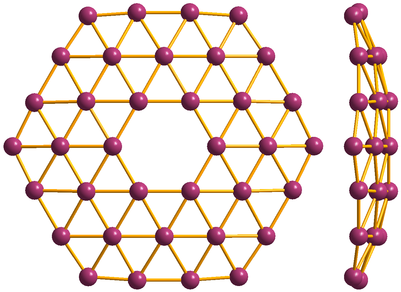
Borophene is a crystalline atomic monolayer of boron, i.e., it is a two-dimensional allotrope of boron and also known as ''boron sheet''.
First predicted by theory in the mid-1990s,
different borophene structures were experimentally confirmed i ...
is a crystalline atomic monolayer of boron and is also known as ''boron sheet''.
First predicted by theory in the mid-1990s in a freestanding state, and then demonstrated as distinct monoatomic layers on substrates by Zhang et al.,
different borophene structures were experimentally confirmed in 2015.
Ge: germanene
Germanene is a two-dimensional allotrope of germanium with a buckled honeycomb structure. Experimentally synthesized germanene exhibits a honeycomb structure. Thishoneycomb
A honeycomb is a mass of hexagonal prismatic wax cells built by honey bees in their nests to contain their larvae and stores of honey and pollen.
Beekeepers may remove the entire honeycomb to harvest honey. Honey bees consume about of honey t ...
structure consists of two hexagon
In geometry, a hexagon (from Greek , , meaning "six", and , , meaning "corner, angle") is a six-sided polygon. The total of the internal angles of any simple (non-self-intersecting) hexagon is 720°.
Regular hexagon
A ''regular hexagon'' h ...
al sub-lattices that are vertically displaced by 0.2 A from each other.
Si: silicene
 Silicene is a two-dimensional allotrope of silicon, with a hexagonal honeycomb structure similar to that of graphene. Its growth is scaffolded by a pervasive Si/Ag(111) surface alloy beneath the two-dimensional layer.
Sn: stanene

Stanene
Stanene is a topological insulator, theoretically predicted by Prof. Shoucheng Zhang's group at Stanford, which may display dissipationless currents at its edges near room temperature. It is composed of tin atoms arranged in a single layer, in a ...
is a predicted topological insulator that may display dissipationless currents at its edges near room temperature. It is composed of tin atoms arranged in a single layer, in a manner similar to graphene. Its buckled structure leads to high reactivity against common air pollutants such as NOx and COx and it is able to trap and dissociate them at low temperature.
A structure determination of stanene using low energy electron diffraction has shown ultra-flat stanene on a Cu(111) surface.
Pb: plumbene
Plumbene
Plumbene is a material made up of a single layer of lead atoms. The material is created in a process similar to that of graphene, silicene, germanene, and stanene, in which high vacuum and high temperature are used to deposit a layer of lead atoms ...
is a two-dimensional allotrope of lead
Lead is a chemical element with the Symbol (chemistry), symbol Pb (from the Latin ) and atomic number 82. It is a heavy metals, heavy metal that is density, denser than most common materials. Lead is Mohs scale of mineral hardness#Intermediate ...
, with a hexagonal honeycomb structure similar to that of graphene.
P: phosphorene
 Phosphorene is a 2-dimensional, crystalline allotrope of phosphorus. Its mono-atomic hexagonal structure makes it conceptually similar to graphene. However, phosphorene has substantially different electronic properties; in particular it possesses a nonzero band gap while displaying high electron mobility. This property potentially makes it a better semiconductor than graphene.
The synthesis of phosphorene mainly consists of micromechanical cleavage or liquid phase exfoliation methods. The former has a low yield while the latter produce free standing nanosheets in solvent and not on the solid support. The bottom-up approaches like chemical vapor deposition (CVD) are still blank because of its high reactivity. Therefore, in the current scenario, the most effective method for large area fabrication of thin films of phosphorene consists of wet assembly techniques like Langmuir-Blodgett involving the assembly followed by deposition of nanosheets on solid supports.
Sb: antimonene
Antimonene is a two-dimensional allotrope of antimony, with its atoms arranged in a buckled honeycomb lattice. Theoretical calculations predicted that antimonene would be a stable semiconductor in ambient conditions with suitable performance for (opto)electronics. Antimonene was first isolated in 2016 by micromechanical exfoliation and it was found to be very stable under ambient conditions. Its properties make it also a good candidate for biomedical and energy applications. In a study made in 2018, antimonene modified screen-printed electrodes (SPE's) were subjected to a galvanostatic charge/discharge test using a two-electrode approach to characterize their supercapacitive properties. The best configuration observed, which contained 36 nanograms of antimonene in the SPE, showed a specific capacitance of 1578 F g−1 at a current of 14 A g−1. Over 10,000 of these galvanostatic cycles, the capacitance retention values drop to 65% initially after the first 800 cycles, but then remain between 65% and 63% for the remaining 9,200 cycles. The 36 ng antimonene/SPE system also showed an energy density of 20 mW h kg−1 and a power density of 4.8 kW kg−1. These supercapacitive properties indicate that antimonene is a promising electrode material for supercapacitor systems. A more recent study, concerning antimonene modified SPEs shows the inherent ability of antimonene layers to form electrochemically passivated layers to facilite electroanalytical measurements in oxygenated environments, in which the presence of dissolved oxygens normally hinders the analytical procedure. The same study also depicts the in-situ production of antimonene oxide/PEDOT:PSS nanocomposites as electrocatalytic platforms for the determination of nitroaromatic compounds.Bi: bismuthene
Bismuthene, the two-dimensional (2D) allotrope of bismuth, was predicted to be a topological insulator. It was predicted that bismuthene retains its topological phase when grown onsilicon carbide
Silicon carbide (SiC), also known as carborundum (), is a hard chemical compound containing silicon and carbon. A semiconductor, it occurs in nature as the extremely rare mineral moissanite, but has been mass-produced as a powder and crystal ...
in 2015. The prediction was successfully realized and synthesized in 2016. At first glance the system is similar to graphene, as the Bi atoms arrange in a honeycomb lattice. However the bandgap is as large as 800mV due to the large spin–orbit interaction (coupling) of the Bi atoms and their interaction with the substrate. Thus, room-temperature applications of the quantum spin Hall effect come into reach. It has been reported to be the largest nontrivial bandgap 2D topological insulator in its natural state. Top-down exfoliation of bismuthene has been reported in various instances with recent works promoting the implementation of bismuthene in the field of electrochemical sensing. Emdadul et al. predicted the mechanical strength and phonon thermal conductivity of monolayer β-bismuthene through atomic-scale analysis. The obtained room temperature (300K) fracture strength is ~4.21 N/m along the armchair direction and ~4.22 N/m along the zigzag direction. At 300 K, its Young's moduli are reported to be ~26.1 N/m and ~25.5 N/m, respectively, along the armchair and zigzag directions. In addition, their predicted phonon thermal conductivity of ~1.3 W/m∙K at 300 K is considerably lower than other analogous 2D honeycombs, making it a promising material for thermoelectric operations.
Metals
platinum
Platinum is a chemical element with the symbol Pt and atomic number 78. It is a dense, malleable, ductile, highly unreactive, precious, silverish-white transition metal. Its name originates from Spanish , a diminutive of "silver".
Pla ...
in a two-dimensional film geometry has been demonstrated. These atomically thin platinum films are epitaxially grown on graphene which imposes a compressive strain that modifies the surface chemistry of the platinum, while also allowing charge transfer through the graphene. Single atom layers of palladium with the thickness down to 2.6 Å, and rhodium with the thickness of less than 4 Å have also been synthesized and characterized with atomic force microscopy and transmission electron microscopy.
2D alloys
Two-dimensional alloys (or surface alloys) are a single atomic layer of alloy that is incommensurate with the underlying substrate. One example is the 2D ordered alloys of Pb with Sn and with Bi. Surface alloys have been found to scaffold two-dimensional layers, as in the case of silicene.2D supracrystals
The supracrystals of 2D materials have been proposed and theoretically simulated. These monolayer crystals are built of supra atomic periodic structures where atoms in the nodes of the lattice are replaced by symmetric complexes. For example, in the hexagonal structure of graphene patterns of 4 or 6 carbon atoms would be arranged hexagonally instead of single atoms, as the repeating node in the unit cell.Compounds
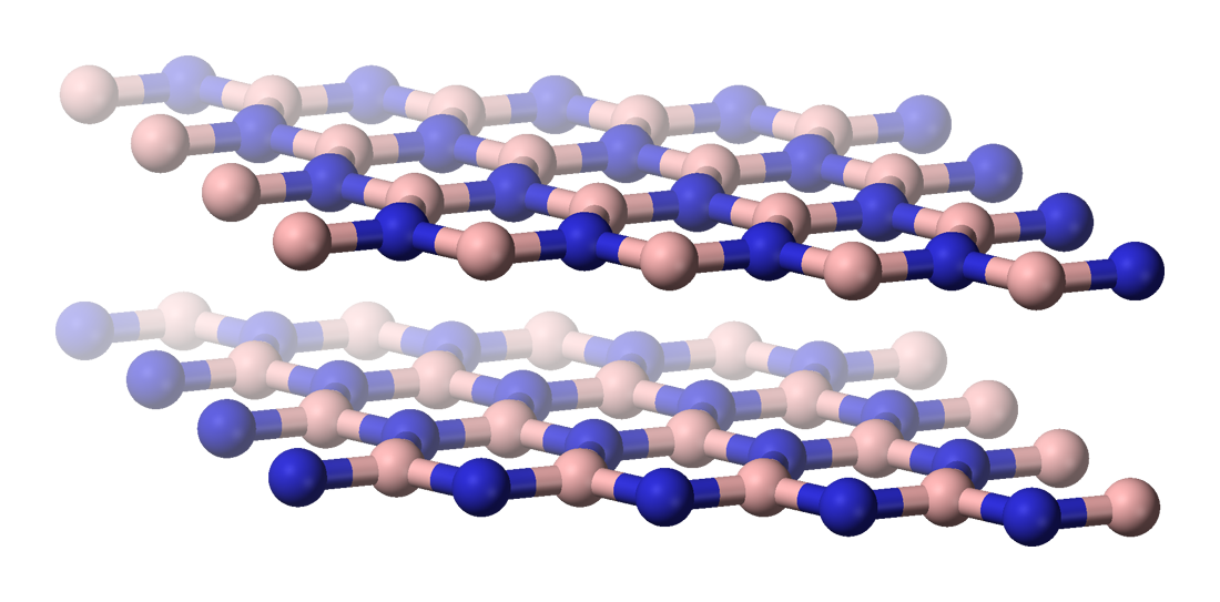
* Boron nitride nanosheet *
*Titanate nanosheet
Titanate (IV) nanosheets (TiNSs) have a 2D structure where TiO6 octahedra are edge-linked in a lepidocrocite-type 2D lattice with chemical formula HxTi2—x/4☐x/4O4 ⦁ H2O (x~0.7; ☐, vacancy).
Titanate nanosheets may be regarded as sheets wi ...
*Borocarbonitrides
Borocarbonitrides are two-dimensional compounds that contain boron, nitrogen, and carbon
Carbon () is a chemical element with the symbol C and atomic number 6. It is nonmetallic and tetravalent
In chemistry, the valence (US spelling) or ...
* MXenes
*2D silica
Two-dimensional silica (2D silica) is a layered polymorph of silicon dioxide. Two varieties of 2D silica, both of hexagonal crystal symmetry, have been grown so far on various metal substrates. One is based on SiO4 tetrahedra, which are covale ...
*Niobium bromide Niobium bromide may refer to
* Niobium(III) bromide. NbBr3
* Niobium(IV) bromide, NbBr4
* Niobium(V) bromide
Niobium(V) bromide is the inorganic compound with the formula Nb2Br10. Its name comes from the compound's empirical formula, NbBr5. It ...
and Niobium chloride ()
Transition metal dichalcogenide monolayers
The most commonly studied two-dimensional transition metal dichalcogenide (TMD) is monolayer molybdenum disulfide (MoS2). Several phases are known, notably the 1T and 2H phases. The naming convention reflects the structure: the 1T phase has one "sheet" (consisting of a layer of S-Mo-S; see figure) per unit cell in a trigonal crystal system, while the 2H phase has two sheets per unit cell in a hexagonal crystal system. The 2H phase is more common, as the 1T phase ismetastable
In chemistry and physics, metastability denotes an intermediate energetic state within a dynamical system other than the system's state of least energy.
A ball resting in a hollow on a slope is a simple example of metastability. If the ball i ...
and spontaneously reverts to 2H without stabilization by additional electron donors (typically surface S vacancies).
 The 2H phase of MoS2 ( Pearson symbol hP6; ''Strukturbericht'' designation C7) has space group P63/mmc. Each layer contains Mo surrounded by S in trigonal prismatic coordination. Conversely, the 1T phase (Pearson symbol hP3) has space group P-3m1, and octahedrally-coordinated Mo; with the 1T unit cell containing only one layer, the unit cell has a ''c'' parameter slightly less than half the length of that of the 2H unit cell (5.95 Å and 12.30 Å, respectively). The different crystal structures of the two phases result in differences in their electronic band structure as well. The d-orbitals of 2H-MoS2 are split into three bands: d''z''2, dx2-y2,xy, and dxz,yz. Of these, only the dz2 is filled; this combined with the splitting results in a semiconducting material with a bandgap of 1.9eV. 1T-MoS2, on the other hand, has partially filled d-orbitals which give it a metallic character.
Because the structure consists of in-plane covalent bonds and inter-layer
 van der Waals interactions
A van is a type of road vehicle used for transporting goods or people. Depending on the type of van, it can be bigger or smaller than a pickup truck and SUV, and bigger than a common car. There is some varying in the scope of the word across th ...
, the electronic properties of monolayer TMDs are highly anisotropic. For example, the conductivity of MoS2 in the direction parallel to the planar layer (0.1–1 ohm-1cm-1) is ~2200 times larger than the conductivity perpendicular to the layers. There are also differences between the properties of a monolayer compared to the bulk material: the Hall mobility
In solid-state physics, the electron mobility characterises how quickly an electron can move through a metal or semiconductor when pulled by an electric field. There is an analogous quantity for holes, called hole mobility. The term carrier mobili ...
at room temperature is drastically lower for monolayer 2H MoS2 (0.1–10 cm2V-1s-1) than for bulk MoS2 (100–500 cm2V-1s-1). This difference arises primarily due to charge traps between the monolayer and the substrate it is deposited on.
MoS2 has important applications in (electro)catalysis. As with other two-dimensional materials, properties can be highly geometry-dependent; the surface of MoS2 is catalytically inactive, but the edges can act as active sites for catalyzing reactions. For this reason, device engineering and fabrication may involve considerations for maximizing catalytic surface area, for example by using small nanoparticles rather than large sheets or depositing the sheets vertically rather than horizontally. Catalytic efficiency also depends strongly on the phase: the aforementioned electronic properties of 2H MoS2 make it a poor candidate for catalysis applications, but these issues can be circumvented through a transition to the metallic (1T) phase. The 1T phase has more suitable properties, with a current density of 10 mA/cm2, an overpotential of –187 mV relative to RHE, and a Tafel slope of 43 mV/decade (compared to 94 mV/decade for the 2H phase).
Graphane
 While graphene has a hexagonal honeycomb lattice structure with alternating double-bonds emerging from its sp2-bonded carbons, graphane, still maintaining the hexagonal structure, is the fully hydrogenated version of graphene with every sp3-hybrized carbon bonded to a hydrogen (chemical formula of (CH)n). Furthermore, while graphene is planar due to its double-bonded nature, graphane is rugged, with the hexagons adopting different out-of-plane structural conformers like the chair or boat, to allow for the ideal 109.5° angles which reduce ring strain, in a direct analogy to the conformers of cyclohexane. Graphane was first theorized in 2003, was shown to be stable using first principles energy calculations in 2007, and was first experimentally synthesized in 2009. There are various experimental routes available for making graphane, including the top-down approaches of reduction of graphite in solution or hydrogenation of graphite using plasma/hydrogen gas as well as the bottom-up approach of chemical vapor deposition. Graphane is an insulator, with a predicted band gap of 3.5 eV; however, partially hydrogenated graphene is a semi-conductor, with the band gap being controlled by the degree of hydrogenation.
;Germanane
Germanane is a single-layer crystal composed of germanium with one hydrogen bonded in the z-direction for each atom. Germanane's structure is similar to graphane, Bulk germanium does not adopt this structure. Germanane is produced in a two-step route starting with
 calcium germanide
Calcium is a chemical element with the symbol Ca and atomic number 20. As an alkaline earth metal, calcium is a reactive metal that forms a dark oxide-nitride layer when exposed to air. Its physical and chemical properties are most similar ...
. From this material, the calcium
Calcium is a chemical element with the symbol Ca and atomic number 20. As an alkaline earth metal, calcium is a reactive metal that forms a dark oxide-nitride layer when exposed to air. Its physical and chemical properties are most similar t ...
(Ca) is removed by de-intercalation
Intercalation may refer to:
* Intercalation (chemistry), insertion of a molecule (or ion) into layered solids such as graphite
*Intercalation (timekeeping), insertion of a leap day, week or month into some calendar years to make the calendar foll ...
with HCl to give a layered solid with the empirical formula GeH. The Ca sites in Zintl-phase CaGe2 interchange with the hydrogen atoms in the HCl solution, producing GeH and CaCl2.
Combined surface alloying
Often single-layer materials, specifically elemental allotrops, are connected to the supporting substrate via surface alloys. By now, this phenomena has been proven via a combination of different measurement techniques for silicene, for which the alloy is difficult to prove by a single technique, and hence has not been expected for a long time. Hence, such scaffolding surface alloys beneath two-dimensional materials can be also expected below other two-dimensional materials, significantly influencing the properties of the two-dimensional layer. During growth, the alloy acts as both, foundation and scaffold for the two-dimensional layer, for which it paves the way.Organic
Ni3(HITP)2 is an organic, crystalline, structurally tunable electrical conductor with a high surface area. HITP is an organic chemical (2,3,6,7,10,11-hexaamino triphenylene). It shares graphene's hexagonalhoneycomb
A honeycomb is a mass of hexagonal prismatic wax cells built by honey bees in their nests to contain their larvae and stores of honey and pollen.
Beekeepers may remove the entire honeycomb to harvest honey. Honey bees consume about of honey t ...
structure. Multiple layers naturally form perfectly aligned stacks, with identical 2-nm openings at the centers of the hexagons. Room temperature electrical conductivity is ~40 S cm−1, comparable to that of bulk graphite and among the highest for any conducting metal-organic frameworks (MOFs). The temperature dependence of its conductivity is linear at temperatures between 100 K and 500 K, suggesting an unusual charge transport mechanism that has not been previously observed in organic semiconductors.
The material was claimed to be the first of a group formed by switching metals and/or organic compounds. The material can be isolated as a powder or a film with conductivity values of 2 and 40 S cm−1, respectively.
Polymer
Using melamine (carbon and nitrogen ring structure) as a monomer, researchers created 2DPA-1, a 2-dimensional polymer sheet held together byhydrogen bond
In chemistry, a hydrogen bond (or H-bond) is a primarily electrostatic force of attraction between a hydrogen (H) atom which is covalently bound to a more electronegative "donor" atom or group (Dn), and another electronegative atom bearing ...
s. The sheet forms spontaneously in solution, allowing thin films to be spin-coated. The polymer has a yield strength twice that of steel, and it resists six times more deformation force than bulletproof glass. It is impermeable to gases and liquids.
Combinations
Single layers of 2D materials can be combined into layered assemblies. For example, bilayer graphene is a material consisting of two layers ofgraphene
Graphene () is an allotrope of carbon consisting of a Single-layer materials, single layer of atoms arranged in a hexagonal lattice nanostructure.
. One of the first reports of bilayer graphene was in the seminal 2004 '' Science (journal), Science'' paper by Geim and colleagues, in which they described devices "which contained just one, two, or three atomic layers". Layered combinations of different 2D materials are generally called van der Waals heterostructures. Twistronics is the study of how the angle (the twist) between layers of two-dimensional materials can change their electrical properties.
Characterization
Microscopy techniques such astransmission electron microscopy
Transmission electron microscopy (TEM) is a microscopy technique in which a beam of electrons is transmitted through a specimen to form an image. The specimen is most often an ultrathin section less than 100 nm thick or a suspension on a gr ...
, 3D electron diffraction, scanning probe microscopy, scanning tunneling microscope, and atomic-force microscopy are used to characterize the thickness and size of the 2D materials. Electrical properties and structural properties such as composition and defects are characterized by Raman spectroscopy, X-ray diffraction, and X-ray photoelectron spectroscopy.
Mechanical characterization
The mechanical characterization of 2D materials is difficult due to ambient reactivity and substrate constraints present in many 2D materials. To this end, many mechanical properties are calculated usingmolecular dynamics
Molecular dynamics (MD) is a computer simulation method for analyzing the physical movements of atoms and molecules. The atoms and molecules are allowed to interact for a fixed period of time, giving a view of the dynamic "evolution" of th ...
simulations or molecular mechanics simulations. Experimental mechanical characterization is possible in 2D materials which can survive the conditions of the experimental setup as well as can be deposited on suitable substrates or exist in a free-standing form. Many 2D materials also possess out-of-plane deformation which further convolute measurements.
Nanoindentation testing is commonly used to experimentally measure elastic modulus, hardness
In materials science, hardness (antonym: softness) is a measure of the resistance to localized plastic deformation induced by either mechanical indentation or abrasion (mechanical), abrasion. In general, different materials differ in their hardn ...
, and fracture strength of 2D materials. From these directly measured values, models exist which allow the estimation of fracture toughness
In materials science, fracture toughness is the critical stress intensity factor of a sharp crack where propagation of the crack suddenly becomes rapid and unlimited. A component's thickness affects the constraint conditions at the tip of a ...
, work hardening exponent, residual stress, and yield strength
In materials science and engineering, the yield point is the point on a stress-strain curve that indicates the limit of Elasticity (physics), elastic behavior and the beginning of Plasticity (physics), plastic behavior. Below the yield point, ...
. These experiments are ran using dedicated nanoindentation equipment or an Atomic Force Microscope (AFM). Nanoindentation experiments are generally ran with the 2D material as a linear strip clamped on both ends experiencing indentation by a wedge, or with the 2D material as a circular membrane clamped around the circumference experiencing indentation by a curbed tip in the center. The strip geometry is difficult to prepare but allows for easier analysis due to linear resulting stress fields. The circular drum-like geometry is more commonly used and can be easily prepared by exfoliating samples onto a patterned substrate. The stress applied to the film in the clamping process can be is refereed to as the residual stress. In the case of very thin layers of 2D materials bending stress is generally ignored in indentation measurements, with bending stress becoming relevant in multilayer samples. Elastic modulus and residual stress values can be extracted by determining the linear and cubic portions of the experimental force-displacement curve. The fracture stress of the 2D sheet is extracted from the applied stress at failure of the sample. AFM tip size was found to have little effect on elastic property measurement, but the breaking force was found to have a strong tip size dependence due stress concentration at the apex of the tip. Using these techniques the elastic modulus and yield strength of graphene were found to be 342 N/m and 55 N/m respectively.
Poisson's ratio measurements in 2D materials is generally straightforward. To get a value, a 2D sheet is placed under stress and displacement responses are measured, or an MD calculation is ran. The unique structures found in 2D materials have been found to result in auxetic
Auxetics are structures or materials that have a negative Poisson's ratio. When stretched, they become thicker perpendicular to the applied force. This occurs due to their particular internal structure and the way this deforms when the sample ...
behavior in phosphorene and graphene and a Poisson's ratio of zero in triangular lattice borophene.
Shear modulus
In materials science, shear modulus or modulus of rigidity, denoted by ''G'', or sometimes ''S'' or ''μ'', is a measure of the elastic shear stiffness of a material and is defined as the ratio of shear stress to the shear strain:
:G \ \stack ...
measurements of graphene has been extracted by measuring a resonance frequency shift in a double paddle oscillator experiment as well as with MD simulations.
Fracture toughness
In materials science, fracture toughness is the critical stress intensity factor of a sharp crack where propagation of the crack suddenly becomes rapid and unlimited. A component's thickness affects the constraint conditions at the tip of a ...
of 2D materials in Mode I (KIC) has been measured directly by stretching pre-cracked layers and monitoring crack propagation in real-time. MD simulations as well as molecular mechanics simulations have also been used to calculate fracture toughness in Mode I. In anisotropic materials, such as phosphorene, crack propagation was found to happen preferentially along certain directions. Most 2D materials were found to undergo brittle fracture.
Applications
The major expectation held amongst researchers is that given their exceptional properties, 2D materials will replace conventional semiconductors to deliver a new generation of electronics.Biological applications
Research on 2D nanomaterials is still in its infancy, with the majority of research focusing on elucidating the unique material characteristics and few reports focusing on biomedical applications of 2D nanomaterials. Nevertheless, recent rapid advances in 2D nanomaterials have raised important yet exciting questions about their interactions withbiological
Biology is the scientific study of life. It is a natural science with a broad scope but has several unifying themes that tie it together as a single, coherent field. For instance, all organisms are made up of cells that process hereditary ...
moieties. 2D nanoparticles such as carbon-based 2D materials, silicate clays, transition metal dichalcogenides (TMDs), and transition metal oxides (TMOs) provide enhanced physical, chemical, and biological functionality owing to their uniform shapes, high surface-to-volume ratios, and surface charge.
Two-dimensional (2D) nanomaterials are ultrathin nanomaterials with a high degree of anisotropy and chemical functionality. 2D nanomaterials are highly diverse in terms of their mechanical, chemical, and optical
Optics is the branch of physics that studies the behaviour and properties of light, including its interactions with matter and the construction of instruments that use or detect it. Optics usually describes the behaviour of visible, ultrav ...
properties, as well as in size, shape, biocompatibility, and degradability. These diverse properties make 2D nanomaterials suitable for a wide range of applications, including drug delivery, imaging
Imaging is the representation or reproduction of an object's form; especially a visual representation (i.e., the formation of an image).
Imaging technology is the application of materials and methods to create, preserve, or duplicate images.
...
, tissue engineering, biosensors, and gas sensors among others. However, their low-dimension nanostructure gives them some common characteristics. For example, 2D nanomaterials are the thinnest materials known, which means that they also possess the highest specific surface areas of all known materials. This characteristic makes these materials invaluable for applications requiring high levels of surface interactions on a small scale. As a result, 2D nanomaterials are being explored for use in drug delivery systems, where they can adsorb large numbers of drug molecules and enable superior control over release kinetics. Additionally, their exceptional surface area to volume ratios and typically high modulus values make them useful for improving the mechanical properties of biomedical nanocomposites
Nanocomposite is a multiphase solid material where one of the phases has one, two or three dimensions of less than 100 nanometers (nm) or structures having nano-scale repeat distances between the different phases that make up the material.
The i ...
and nanocomposite hydrogels, even at low concentrations. Their extreme thinness has been instrumental for breakthroughs in biosensing and gene sequencing Gene Sequencing may refer to:
* DNA sequencing
* or a comprehensive variant of it: Whole genome sequencing
Whole genome sequencing (WGS), also known as full genome sequencing, complete genome sequencing, or entire genome sequencing, is the pro ...
. Moreover, the thinness of these molecules allows them to respond rapidly to external signals such as light, which has led to utility in optical therapies of all kinds, including imaging applications, photothermal therapy (PTT), and photodynamic therapy (PDT).
Despite the rapid pace of development in the field of 2D nanomaterials, these materials must be carefully evaluated for biocompatibility in order to be relevant for biomedical applications. The newness of this class of materials means that even the relatively well-established 2D materials like graphene
Graphene () is an allotrope of carbon consisting of a Single-layer materials, single layer of atoms arranged in a hexagonal lattice nanostructure.
are poorly understood in terms of their physiological interactions with living tissue (biology), tissues. Additionally, the complexities of variable particle size and shape, impurities from manufacturing, and protein
Proteins are large biomolecules and macromolecules that comprise one or more long chains of amino acid residues. Proteins perform a vast array of functions within organisms, including catalysing metabolic reactions, DNA replication, respon ...
and immune interactions have resulted in a patchwork of knowledge on the biocompatibility of these materials.
See also
* Monolayer * Two-dimensional semiconductor * Transition metal dichalcogenide monolayersReferences
Additional reading
* * * * * * *{{cite journal, last1=Kolesnichenko, first1=Pavel, last2=Zhang, first2=Qianhui, last3=Zheng, first3=Changxi, last4=Fuhrer, first4=Michael, last5=Davis, first5=Jeffrey, date=2021, title=Multidimensional analysis of excitonic spectra of monolayers of tungsten disulphide: toward computer-aided identification of structural and environmental perturbations of 2D materials, journal=Machine Learning: Science and Technology, volume=2, issue=2, pages=025021, doi=10.1088/2632-2153/abd87c, doi-access=free * Condensed matter physics Semiconductors Monolayers