|
Lab-on-chip
A lab-on-a-chip (LOC) is a device that integrates one or several laboratory functions on a single integrated circuit (commonly called a "chip") of only millimeters to a few square centimeters to achieve automation and high-throughput screening. LOCs can handle extremely small fluid volumes down to less than pico-liters. Lab-on-a-chip devices are a subset of microelectromechanical systems (MEMS) devices and sometimes called "micro total analysis systems" (μTAS). LOCs may use microfluidics, the physics, manipulation and study of minute amounts of fluids. However, strictly regarded "lab-on-a-chip" indicates generally the scaling of single or multiple lab processes down to chip-format, whereas "μTAS" is dedicated to the integration of the total sequence of lab processes to perform chemical analysis. History After the invention of microtechnology (≈1954) for realizing integrated semiconductor structures for microelectronic chips, these lithography-based technologies were soon a ... [...More Info...] [...Related Items...] OR: [Wikipedia] [Google] [Baidu] |
Off-stoichiometry Thiol-ene Polymer
An off-stoichiometry thiol-ene polymer is a polymer platform comprising off-stoichiometry thiol-enes (OSTE) and off-stoichiometry thiol-ene-epoxies (OSTE+). The OSTE polymers comprise off-stoichiometry blends of thiols and allyls. After complete polymerization, typically by UV micromolding, the polymer articles contain a well-defined number of unreacted thiol or allyls groups both on the surface and in the bulk. These surface anchors can be used for subsequent direct surface modification or bonding. In later versions epoxy monomers were added to form ternary thiol-ene-epoxy monomer systems (OSTE+), where the epoxy in a second step reacts with the excess of thiols creating a final polymer article that is completely inert. Some of the critical features of OSTE+ polymers include uncomplicated and rapid fabrication of complex structures in a standard chemistry labs, hydrophilic native surface properties and covalent bonding via latent epoxy chemistry. Development The OSTE polymer res ... [...More Info...] [...Related Items...] OR: [Wikipedia] [Google] [Baidu] |
DNA Microarrays
A DNA microarray (also commonly known as a DNA chip or biochip) is a collection of microscopic DNA spots attached to a solid surface. Scientists use DNA microarrays to measure the expression levels of large numbers of genes simultaneously or to genotype multiple regions of a genome. Each DNA spot contains picomoles (10−12 moles) of a specific DNA sequence, known as '' probes'' (or ''reporters'' or '' oligos''). These can be a short section of a gene or other DNA element that are used to hybridize a cDNA or cRNA (also called anti-sense RNA) sample (called ''target'') under high-stringency conditions. Probe-target hybridization is usually detected and quantified by detection of fluorophore-, silver-, or chemiluminescence-labeled targets to determine relative abundance of nucleic acid sequences in the target. The original nucleic acid arrays were macro arrays approximately 9 cm × 12 cm and the first computerized image based analysis was published in 1981. It was inv ... [...More Info...] [...Related Items...] OR: [Wikipedia] [Google] [Baidu] |
Laboratory
A laboratory (; ; colloquially lab) is a facility that provides controlled conditions in which scientific or technological research, experiments, and measurement may be performed. Laboratories are found in a variety of settings such as schools, universities, privately owned research institutions, corporate research and testing facilities, government regulatory and forensic investigation centers, physicians' offices, clinics, hospitals, regional and national referral centers, and even occasionally personal residences. Overview The organisation and contents of laboratories are determined by the differing requirements of the specialists working within. A physics laboratory might contain a particle accelerator or vacuum chamber, while a metallurgy laboratory could have apparatus for casting or refining metals or for testing their strength. A chemist or biologist might use a wet laboratory, while a psychologist's laboratory might be a room with one-way mirrors and hidden ... [...More Info...] [...Related Items...] OR: [Wikipedia] [Google] [Baidu] |
Capillary Electrophoresis
Capillary electrophoresis (CE) is a family of electrokinetic separation methods performed in submillimeter diameter capillaries and in micro- and nanofluidic channels. Very often, CE refers to capillary zone electrophoresis (CZE), but other electrophoresis, electrophoretic techniques including capillary gel electrophoresis (CGE), capillary isoelectric focusing (CIEF), capillary isotachophoresis and micellar electrokinetic chromatography (MEKC) belong also to this class of methods. In CE methods, analytes migrate through electrolyte solutions under the influence of an electric field. Analytes can be separated according to ionic mobility and/or partitioning into an alternate phase via non-covalent interactions. Additionally, analytes may be concentrated or "focused" by means of gradients in Electrical resistivity and conductivity, conductivity and pH. Instrumentation The instrumentation needed to perform capillary electrophoresis is relatively simple. A basic schematic of a capil ... [...More Info...] [...Related Items...] OR: [Wikipedia] [Google] [Baidu] |
Stereolithography
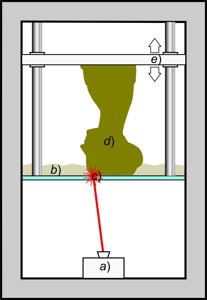
Stereolithography (SLA or SL; also known as vat photopolymerisation, optical fabrication, photo-solidification, or resin printing) is a form of 3D printing technology used for creating models, prototypes, patterns, and production parts in a layer by layer fashion using photochemical processes by which light causes chemical monomers and oligomers to cross-link together to form polymers. U.S. Patentbr>4,575,330(“Apparatus for Production of Three-Dimensional Objects by Stereolithography”) Those polymers then make up the body of a three-dimensional solid. Research in the area had been conducted during the 1970s, but the term was coined by Chuck Hull in 1984 when he applied for a patent on the process, which was granted in 1986. Stereolithography can be used to create prototypes for products in development, medical models, and computer hardware, as well as in many other applications. While stereolithography is fast and can produce almost any design, it can be expensive. History ... [...More Info...] [...Related Items...] OR: [Wikipedia] [Google] [Baidu] |
Soft Lithography
In technology, soft lithography is a family of techniques for fabricating or Replication (other), replicating structures using "elastomeric stamps, molds, and conformable photomasks". It is called "soft" because it uses elastomeric materials, most notably Polydimethylsiloxane, PDMS. Soft lithography is generally used to construct features measured on the micrometer to nanometer Scale (measurement), scale. According to Rogers and Nuzzo (2005), Research and development, development of soft lithography expanded rapidly from 1995 to 2005. Soft lithography tools are now commercially available. Types * PDMS stamp * Microcontact printing * Multilayer soft lithography * Nanosphere lithography * Patterning by etching at the nanoscale Advantages Soft lithography has some unique advantages over other forms of lithography (such as photolithography and electron beam lithography). They include the following: *Lower cost than traditional photolithography in mass production *Well- ... [...More Info...] [...Related Items...] OR: [Wikipedia] [Google] [Baidu] |
Polydimethylsiloxane
Polydimethylsiloxane (PDMS), also known as dimethylpolysiloxane or dimethicone, is a silicone polymer with a wide variety of uses, from cosmetics to industrial lubrication and passive daytime radiative cooling. PDMS is particularly known for its unusual rheological (or flow) properties. It is optically clear and, in general, inert, non-toxic, and non-flammable. It is one of several types of silicone oil (polymerized siloxane). The applications of PDMS range from contact lenses and medical devices to elastomers; it is also present in shampoos (as it makes hair shiny and slippery), food ( antifoaming agent), caulk, lubricants and heat-resistant tiles. Structure The chemical formula of PDMS is , where ''n'' is the number of repeating monomer units. Industrial synthesis can begin from dimethyldichlorosilane and water by the following net reaction: : + (''n''+1) The polymerization reaction evolves hydrochloric acid. For medical and domestic applications, a process wa ... [...More Info...] [...Related Items...] OR: [Wikipedia] [Google] [Baidu] |
Industrial Etching
Chemical milling or industrial etching is the subtractive manufacturing process of using baths of temperature-regulated etching chemicals to remove material to create an object with the desired shape. Other names for chemical etching include photo etching, chemical etching, photo chemical etching and photochemical machining. It is mostly used on metals, though other materials are increasingly important. It was developed from armor-decorating and printing etching processes developed during the Renaissance as alternatives to engraving on metal. The process essentially involves bathing the cutting areas in a corrosive chemical known as an etchant, which reacts with the material in the area to be cut and causes the solid material to be dissolved; inert substances known as maskants are used to protect specific areas of the material as resists. History Organic chemicals such as lactic acid and citric acid have been used to etch metals and create products as early as 400 BCE ... [...More Info...] [...Related Items...] OR: [Wikipedia] [Google] [Baidu] |
Photolithography
Photolithography (also known as optical lithography) is a process used in the manufacturing of integrated circuits. It involves using light to transfer a pattern onto a substrate, typically a silicon wafer. The process begins with a photosensitive material, called a photoresist, being applied to the substrate. A photomask that contains the desired pattern is then placed over the photoresist. Light is shone through the photomask, exposing the photoresist in certain areas. The exposed areas undergo a chemical change, making them either soluble or insoluble in a developer solution. After development, the pattern is transferred onto the substrate through etching, chemical vapor deposition, or ion implantation processes. Ultraviolet, Ultraviolet (UV) light is typically used. Photolithography processes can be classified according to the type of light used, including ultraviolet lithography, deep ultraviolet lithography, extreme ultraviolet lithography, extreme ultraviolet lithography ... [...More Info...] [...Related Items...] OR: [Wikipedia] [Google] [Baidu] |
Springer Verlag
Springer Science+Business Media, commonly known as Springer, is a German multinational publishing company of books, e-books and peer-reviewed journals in science, humanities, technical and medical (STM) publishing. Originally founded in 1842 in Berlin, it expanded internationally in the 1960s, and through mergers in the 1990s and a sale to venture capitalists it fused with Wolters Kluwer and eventually became part of Springer Nature in 2015. Springer has major offices in Berlin, Heidelberg, Dordrecht, and New York City. History Julius Springer founded Springer-Verlag in Berlin in 1842 and his son Ferdinand Springer grew it from a small firm of 4 employees into Germany's then second-largest academic publisher with 65 staff in 1872.Chronology ". Springer Science+Business Media. In 1964, Springer expanded its business internationally, op ... [...More Info...] [...Related Items...] OR: [Wikipedia] [Google] [Baidu] |
Nanotechnology
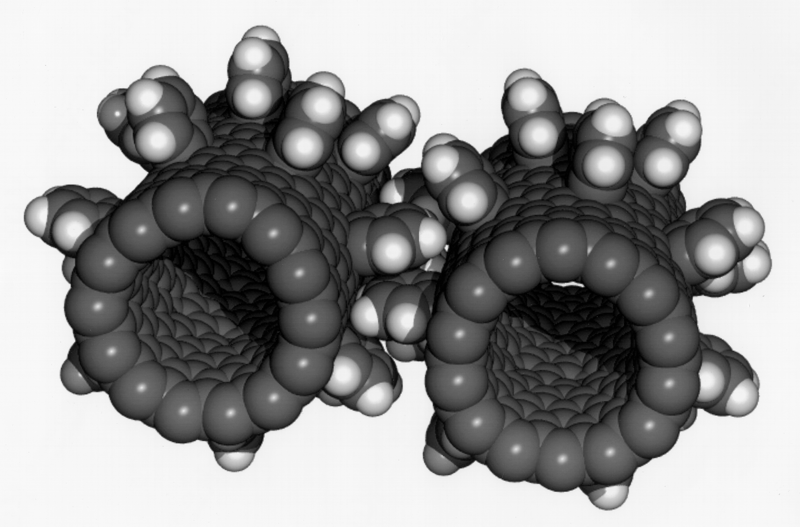
Nanotechnology is the manipulation of matter with at least one dimension sized from 1 to 100 nanometers (nm). At this scale, commonly known as the nanoscale, surface area and quantum mechanical effects become important in describing properties of matter. This definition of nanotechnology includes all types of research and technologies that deal with these special properties. It is common to see the plural form "nanotechnologies" as well as "nanoscale technologies" to refer to research and applications whose common trait is scale. An earlier understanding of nanotechnology referred to the particular technological goal of precisely manipulating atoms and molecules for fabricating macroscale products, now referred to as molecular nanotechnology. Nanotechnology defined by scale includes fields of science such as surface science, organic chemistry, molecular biology, semiconductor physics, energy storage, engineering, microfabrication, and molecular engineering. The associated rese ... [...More Info...] [...Related Items...] OR: [Wikipedia] [Google] [Baidu] |
Cellomics
Cellomics is the discipline of quantitative cell analysis using bioimaging methods and informatics with a workflow involving three major components: image acquisition, image analysis, and data visualization and management. These processes are generally automated. All three of these components depend on sophisticated software to acquire qualitative data, quantitative data, and the management of both images and data, respectively. Cellomics is also a trademarked term, which is often used interchangeably with high-content analysis (HCA) or high-content screening (HCS), but cellomics extends beyond HCA/HCS by incorporating sophisticated informatics tools. History HCS and the discipline of cellomics was pioneered by a once privately held company named Cellomics Inc., which commercialized instruments, software, and reagents to facilitate the study of cells in culture, and more specifically, their responses to potentially therapeutic drug-like molecules. In 2005, Cellomics was acquire ... [...More Info...] [...Related Items...] OR: [Wikipedia] [Google] [Baidu] |


