|
Lab-on-a-chip
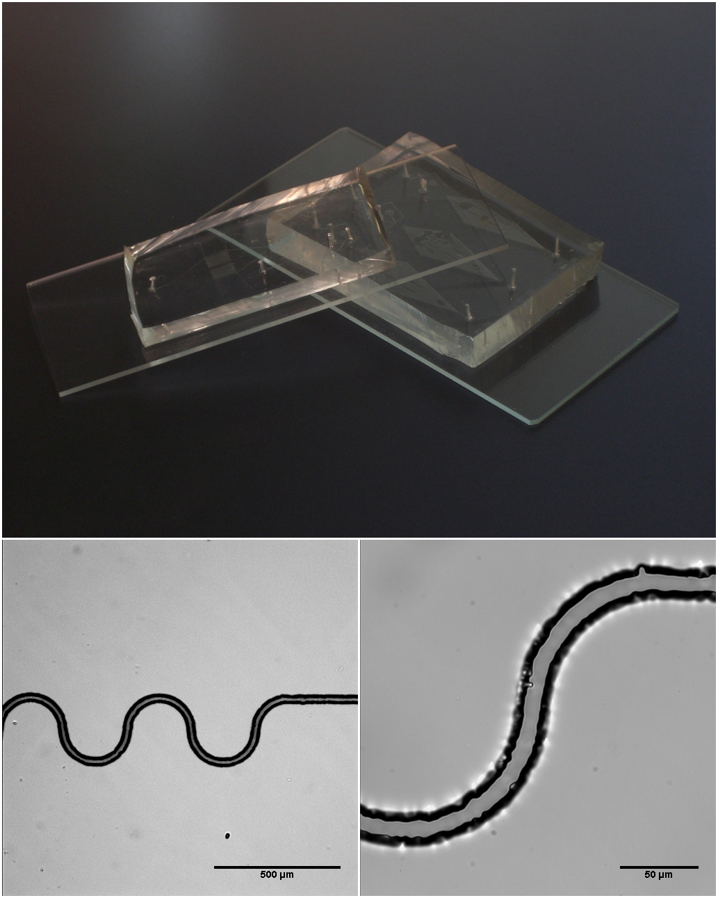
A lab-on-a-chip (LOC) is a device that integrates one or several laboratory functions on a single integrated circuit (commonly called a "chip") of only millimeters to a few square centimeters to achieve automation and high-throughput screening. LOCs can handle extremely small fluid volumes down to less than pico-liters. Lab-on-a-chip devices are a subset of microelectromechanical systems (MEMS) devices and sometimes called "micro total analysis systems" (μTAS). LOCs may use microfluidics, the physics, manipulation and study of minute amounts of fluids. However, strictly regarded "lab-on-a-chip" indicates generally the scaling of single or multiple lab processes down to chip-format, whereas "μTAS" is dedicated to the integration of the total sequence of lab processes to perform chemical analysis. History After the invention of microtechnology (≈1954) for realizing integrated semiconductor structures for microelectronic chips, these lithography-based technologies were soon ... [...More Info...] [...Related Items...] OR: [Wikipedia] [Google] [Baidu] |
Off-stoichiometry Thiol-ene Polymer
An off-stoichiometry thiol-ene polymer is a polymer platform comprising off-stoichiometry thiol-enes (OSTE) and off-stoichiometry thiol-ene-epoxies (OSTE+). The OSTE polymers comprise off-stoichiometry blends of thiols and allyls. After complete polymerization, typically by UV micromolding, the polymer articles contain a well-defined number of unreacted thiol or allyls groups both on the surface and in the bulk. These surface anchors can be used for subsequent direct surface modification or bonding. In later versions epoxy monomers were added to form ternary thiol-ene-epoxy monomer systems (OSTE+), where the epoxy in a second step reacts with the excess of thiols creating a final polymer article that is completely inert. Some of the critical features of OSTE+ polymers include uncomplicated and rapid fabrication of complex structures in a standard chemistry labs, hydrophilic native surface properties and covalent bonding via latent epoxy chemistry. Development The OSTE polymer res ... [...More Info...] [...Related Items...] OR: [Wikipedia] [Google] [Baidu] |
Total Analysis System
The term total analysis system (TAS) describes a device that combines and automates all necessary steps for the chemical analysis of a sample (e.g., sampling, sample transport, filtration, dilution, chemical reactions, separation, and detection). Most current total analysis systems are "micro" total analysis systems which utilize the principles of microfluidics. Total analysis systems are designed to shrink the processes carried out in a laboratory to a chip-sized lab-on-a-chip. Due to this, it can be more cost-effective to carry out complex tests when considering chip technologies, sample sizes, and analysis time. Total analysis systems can also reduce the exposure of toxic chemicals for lab personnel. This technology can also be used in point-of-care testing or point-of-use diagnostics, which do not require skilled technicians. See also *Microelectromechanical systems *Microfluidics *Bio-MEMS *Lab-on-a-chip A lab-on-a-chip (LOC) is a device that integrates one or several lab ... [...More Info...] [...Related Items...] OR: [Wikipedia] [Google] [Baidu] |
Microfluidics
Microfluidics refers to a system that manipulates a small amount of fluids (10−9 to 10−18 liters) using small channels with sizes of ten to hundreds of micrometres. It is a multidisciplinary field that involves molecular analysis, molecular biology, and microelectronics. It has practical applications in the design of systems that process low volumes of fluids to achieve multiplexing, automation, and high-throughput screening. Microfluidics emerged in the beginning of the 1980s and is used in the development of inkjet printheads, DNA chips, lab-on-a-chip technology, micro-propulsion, and micro-thermal technologies. Typically, micro means one of the following features: * Small volumes (μL, nL, pL, fL) * Small size * Low energy consumption * Microdomain effects Typically microfluidic systems transport, mix, separate, or otherwise process fluids. Various applications rely on passive fluid control using capillary forces, in the form of capillary flow modifying elements, akin to f ... [...More Info...] [...Related Items...] OR: [Wikipedia] [Google] [Baidu] |
Microelectromechanical Systems
MEMS (micro-electromechanical systems) is the technology of microscopic devices incorporating both electronic and moving parts. MEMS are made up of components between 1 and 100 micrometres in size (i.e., 0.001 to 0.1 mm), and MEMS devices generally range in size from 20 micrometres to a millimetre (i.e., 0.02 to 1.0 mm), although components arranged in arrays (e.g., digital micromirror devices) can be more than 1000 mm2. They usually consist of a central unit that processes data (an integrated circuit chip such as microprocessor) and several components that interact with the surroundings (such as microsensors). Because of the large surface area to volume ratio of MEMS, forces produced by ambient electromagnetism (e.g., electrostatic charges and magnetic moments), and fluid dynamics (e.g., surface tension and viscosity) are more important design considerations than with larger scale mechanical devices. MEMS technology is distinguished from molecular nanotechnol ... [...More Info...] [...Related Items...] OR: [Wikipedia] [Google] [Baidu] |
Laboratory
A laboratory (; ; colloquially lab) is a facility that provides controlled conditions in which scientific or technological research, experiments, and measurement may be performed. Laboratories are found in a variety of settings such as schools, universities, privately owned research institutions, corporate research and testing facilities, government regulatory and forensic investigation centers, physicians' offices, clinics, hospitals, regional and national referral centers, and even occasionally personal residences. Overview The organisation and contents of laboratories are determined by the differing requirements of the specialists working within. A physics laboratory might contain a particle accelerator or vacuum chamber, while a metallurgy laboratory could have apparatus for casting or refining metals or for testing their strength. A chemist or biologist might use a wet laboratory, while a psychologist's laboratory might be a room with one-way mirrors and hidden ... [...More Info...] [...Related Items...] OR: [Wikipedia] [Google] [Baidu] |
Springer Verlag
Springer Science+Business Media, commonly known as Springer, is a German multinational publishing company of books, e-books and peer-reviewed journals in science, humanities, technical and medical (STM) publishing. Originally founded in 1842 in Berlin, it expanded internationally in the 1960s, and through mergers in the 1990s and a sale to venture capitalists it fused with Wolters Kluwer and eventually became part of Springer Nature in 2015. Springer has major offices in Berlin, Heidelberg, Dordrecht, and New York City. History Julius Springer founded Springer-Verlag in Berlin in 1842 and his son Ferdinand Springer grew it from a small firm of 4 employees into Germany's then second-largest academic publisher with 65 staff in 1872.Chronology ". Springer Science+Business Media. In 1964, Springer expanded its business internationally, op ... [...More Info...] [...Related Items...] OR: [Wikipedia] [Google] [Baidu] |
Biological Warfare
Biological warfare, also known as germ warfare, is the use of biological toxins or Pathogen, infectious agents such as bacteria, viruses, insects, and Fungus, fungi with the intent to kill, harm or incapacitate humans, animals or plants as an act of war. Biological agent, Biological weapons (often termed "bio-weapons", "biological threat agents", or "bio-agents") are living organisms or replicating entities (i.e. viruses, which are not universally considered "alive"). Entomological warfare, Entomological (insect) warfare is a subtype of biological warfare. Biological warfare is subject to a forceful Social norm, normative prohibition. Offensive biological warfare in international armed conflicts is a war crime under the 1925 Geneva Protocol and several international humanitarian law Treaty, treaties. In particular, the 1972 Biological Weapons Convention (BWC) bans the development, production, acquisition, transfer, stockpiling and use of biological weapons. In contrast, Biode ... [...More Info...] [...Related Items...] OR: [Wikipedia] [Google] [Baidu] |
Cellomics
Cellomics is the discipline of quantitative cell analysis using bioimaging methods and informatics with a workflow involving three major components: image acquisition, image analysis, and data visualization and management. These processes are generally automated. All three of these components depend on sophisticated software to acquire qualitative data, quantitative data, and the management of both images and data, respectively. Cellomics is also a trademarked term, which is often used interchangeably with high-content analysis (HCA) or high-content screening (HCS), but cellomics extends beyond HCA/HCS by incorporating sophisticated informatics tools. History HCS and the discipline of cellomics was pioneered by a once privately held company named Cellomics Inc., which commercialized instruments, software, and reagents to facilitate the study of cells in culture, and more specifically, their responses to potentially therapeutic drug-like molecules. In 2005, Cellomics was acquire ... [...More Info...] [...Related Items...] OR: [Wikipedia] [Google] [Baidu] |
Nanotechnology
Nanotechnology is the manipulation of matter with at least one dimension sized from 1 to 100 nanometers (nm). At this scale, commonly known as the nanoscale, surface area and quantum mechanical effects become important in describing properties of matter. This definition of nanotechnology includes all types of research and technologies that deal with these special properties. It is common to see the plural form "nanotechnologies" as well as "nanoscale technologies" to refer to research and applications whose common trait is scale. An earlier understanding of nanotechnology referred to the particular technological goal of precisely manipulating atoms and molecules for fabricating macroscale products, now referred to as molecular nanotechnology. Nanotechnology defined by scale includes fields of science such as surface science, organic chemistry, molecular biology, semiconductor physics, energy storage, engineering, microfabrication, and molecular engineering. The associated rese ... [...More Info...] [...Related Items...] OR: [Wikipedia] [Google] [Baidu] |
Polydimethylsiloxane
Polydimethylsiloxane (PDMS), also known as dimethylpolysiloxane or dimethicone, is a silicone polymer with a wide variety of uses, from cosmetics to industrial lubrication and passive daytime radiative cooling. PDMS is particularly known for its unusual rheological (or flow) properties. It is optically clear and, in general, inert, non-toxic, and non-flammable. It is one of several types of silicone oil (polymerized siloxane). The applications of PDMS range from contact lenses and medical devices to elastomers; it is also present in shampoos (as it makes hair shiny and slippery), food ( antifoaming agent), caulk, lubricants and heat-resistant tiles. Structure The chemical formula of PDMS is , where ''n'' is the number of repeating monomer units. Industrial synthesis can begin from dimethyldichlorosilane and water by the following net reaction: : + (''n''+1) The polymerization reaction evolves hydrochloric acid. For medical and domestic applications, a process wa ... [...More Info...] [...Related Items...] OR: [Wikipedia] [Google] [Baidu] |
Photolithography
Photolithography (also known as optical lithography) is a process used in the manufacturing of integrated circuits. It involves using light to transfer a pattern onto a substrate, typically a silicon wafer. The process begins with a photosensitive material, called a photoresist, being applied to the substrate. A photomask that contains the desired pattern is then placed over the photoresist. Light is shone through the photomask, exposing the photoresist in certain areas. The exposed areas undergo a chemical change, making them either soluble or insoluble in a developer solution. After development, the pattern is transferred onto the substrate through etching, chemical vapor deposition, or ion implantation processes. Ultraviolet, Ultraviolet (UV) light is typically used. Photolithography processes can be classified according to the type of light used, including ultraviolet lithography, deep ultraviolet lithography, extreme ultraviolet lithography, extreme ultraviolet lithography ... [...More Info...] [...Related Items...] OR: [Wikipedia] [Google] [Baidu] |


