Two Dimensional Semiconductors on:
[Wikipedia]
[Google]
[Amazon]
A two-dimensional semiconductor (also known as 2D semiconductor) is a type of natural


 2D semiconductor materials are often synthesized using a
 Some applications include electronic devices, photonic and energy harvesting devices, and flexible and transparent substrates. Other applications include on quantum computing qubit devices solar cells, and flexible electronics.

semiconductor
A semiconductor is a material which has an electrical resistivity and conductivity, electrical conductivity value falling between that of a electrical conductor, conductor, such as copper, and an insulator (electricity), insulator, such as glas ...
with thicknesses on the atomic scale. Geim and Novoselov et al. initiated the field in 2004 when they reported a new semiconducting material graphene
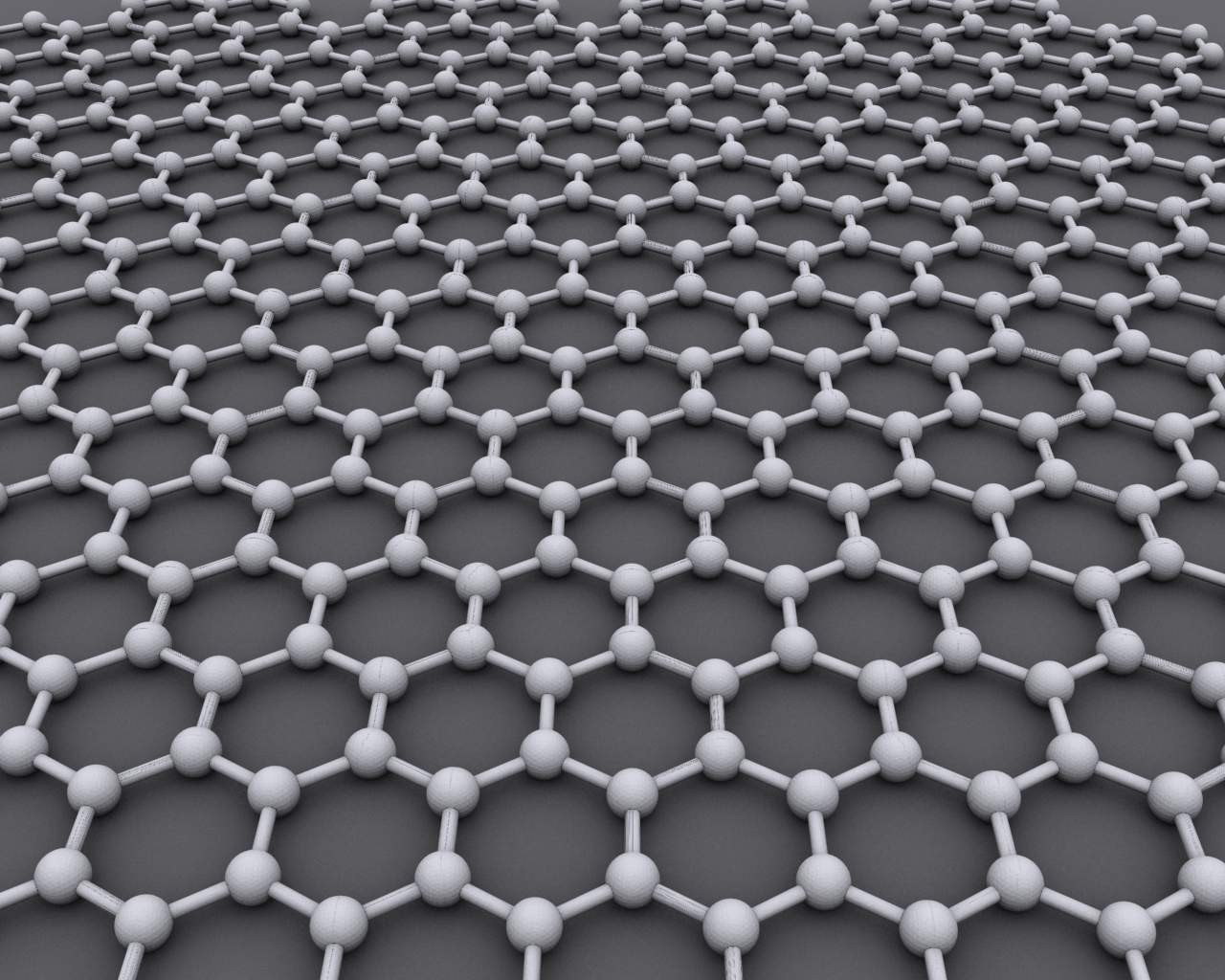
Graphene () is an allotrope of carbon consisting of a single layer of atoms arranged in a hexagonal lattice nanostructure.
, a flat monolayer of carbon atoms arranged in a 2D materials, 2D honeycomb lattice. A 2D monolayer semiconductor is significant because it exhibits stronger piezoelectric coupling than traditionally employed bulk forms. This coupling could enable applications. One research focus is on designing nanoelectronic
Nanoelectronics refers to the use of nanotechnology in electronic components. The term covers a diverse set of devices and materials, with the common characteristic that they are so small that inter-atomic interactions and quantum mechanical pr ...
components by the use of graphene as electrical conductor
In physics and electrical engineering, a conductor is an object or type of material that allows the flow of charge (electric current) in one or more directions. Materials made of metal are common electrical conductors. Electric current is gener ...
, hexagonal boron nitride as electrical insulator
An electrical insulator is a material in which electric current does not flow freely. The atoms of the insulator have tightly bound electrons which cannot readily move. Other materials—semiconductors and conductors—conduct electric current ...
, and a transition metal dichalcogenide as semiconductor
A semiconductor is a material which has an electrical resistivity and conductivity, electrical conductivity value falling between that of a electrical conductor, conductor, such as copper, and an insulator (electricity), insulator, such as glas ...
.
Materials

Graphene
Graphene, consisting of single sheets of carbon atoms, has highelectron mobility
In solid-state physics, the electron mobility characterises how quickly an electron can move through a metal or semiconductor when pulled by an electric field. There is an analogous quantity for holes, called hole mobility. The term carrier mobili ...
and high thermal conductivity
The thermal conductivity of a material is a measure of its ability to conduct heat. It is commonly denoted by k, \lambda, or \kappa.
Heat transfer occurs at a lower rate in materials of low thermal conductivity than in materials of high thermal ...
. One issue regarding graphene is its lack of a band gap
In solid-state physics, a band gap, also called an energy gap, is an energy range in a solid where no electronic states can exist. In graphs of the electronic band structure of solids, the band gap generally refers to the energy difference (in ...
, which poses a problem in particular with digital electronics because it is unable to switch off field-effect transistor
The field-effect transistor (FET) is a type of transistor that uses an electric field to control the flow of current in a semiconductor. FETs (JFETs or MOSFETs) are devices with three terminals: ''source'', ''gate'', and ''drain''. FETs contro ...
s (FETs).
Nanosheets of other group-IV elements (Si, Ge and Sn) present structural and electronic properties similar to graphene.

Hexagonal boron nitride
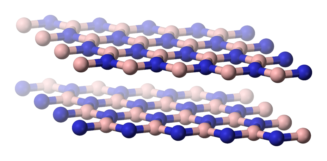
Monolayer hexagonalboron nitride
Boron nitride is a thermally and chemically resistant refractory compound of boron and nitrogen with the chemical formula BN. It exists in various crystalline forms that are isoelectronic to a similarly structured carbon lattice. The hexagonal ...
(h-BN) is an insulator with a high energy gap (5.97 eV). However, it can also function as a semiconductor with enhanced conductivity due to its zigzag sharp edges and vacancies. h-BN is often used as substrate and barrier due to its insulating property. h-BN also has a large thermal conductivity.

Transition-metal dichalcogenides
Transition-metal dichalcogenide monolayers (TMDs or TMDCs) are a class of two-dimensional materials that have the chemical formula MX2, where M representstransition metals
In chemistry, a transition metal (or transition element) is a chemical element in the d-block of the periodic table (groups 3 to 12), though the elements of group 12 (and less often group 3) are sometimes excluded. They are the elements that can ...
from group VI, V and VI, and X represents a chalcogen
The chalcogens (ore forming) ( ) are the chemical elements in group 16 of the periodic table. This group is also known as the oxygen family. Group 16 consists of the elements oxygen (O), sulfur (S), selenium (Se), tellurium (Te), and the radioact ...
such as sulfur
Sulfur (or sulphur in British English) is a chemical element with the symbol S and atomic number 16. It is abundant, multivalent and nonmetallic. Under normal conditions, sulfur atoms form cyclic octatomic molecules with a chemical formula ...
, selenium
Selenium is a chemical element with the symbol Se and atomic number 34. It is a nonmetal (more rarely considered a metalloid) with properties that are intermediate between the elements above and below in the periodic table, sulfur and tellurium, ...
or tellurium
Tellurium is a chemical element with the symbol Te and atomic number 52. It is a brittle, mildly toxic, rare, silver-white metalloid. Tellurium is chemically related to selenium and sulfur, all three of which are chalcogens. It is occasionally fou ...
. MoS2, MoSe2, MoTe2, WS2 and WSe2 are TMDCs. TMDCs have layered structure with a plane of metal atoms in between two planes of chalcogen atoms as shown in Figure 1. Each layer is bonded strongly in plane, but weakly in interlayers. Therefore, TMDCs can be easily exfoliated into atomically thin layers through various methods. TMDCs show layer-dependent optical and electrical properties. When exfoliated into monolayers, the band gaps of several TMDCs change from indirect to direct, which lead to broad applications in nanoelectronics, optoelectronics, and quantum computing
Quantum computing is a type of computation whose operations can harness the phenomena of quantum mechanics, such as superposition, interference, and entanglement. Devices that perform quantum computations are known as quantum computers. Though ...
.
III-IV chalcogenides
Another class of 2D semiconductors are III-IV chalcogenides. These materials have the chemical formula MX, where M is a metal from group 13 ( Ga, In) and X is a chalcogen atom ( S, Se, Te). Typical members of this group are InSe and GaSe, both of which have shown high electronic mobilities and band gaps suitable for a wide range of electronic applications.Synthesis
chemical vapor deposition
Chemical vapor deposition (CVD) is a vacuum deposition method used to produce high quality, and high-performance, solid materials. The process is often used in the semiconductor industry to produce thin films.
In typical CVD, the wafer (substra ...
(CVD) method. Because CVD can provide large-area, high-quality, and well-controlled layered growth of 2D semiconductor materials, it also allows synthesis of two-dimensional heterojunction A heterojunction is an interface between two layers or regions of dissimilar semiconductors. These semiconducting materials have unequal band gaps as opposed to a homojunction. It is often advantageous to engineer the electronic energy bands in many ...
s. When building devices by stacking different 2D materials, mechanical exfoliation followed by transferring is often used. Other possible synthesis methods include chemical exfoliation, hydrothermal synthesis, and thermal decomposition
Thermal decomposition, or thermolysis, is a chemical decomposition caused by heat. The decomposition temperature of a substance is the temperature at which the substance chemically decomposes. The reaction is usually endothermic as heat is req ...
. In 2008 cadmium selenide CdSe quasi 2D platelets were first synthesized by colloidal method with thicknesses of several atomic layers and lateral sizes up to dozens of nanometers. Modification of the procedure allowed to obtain other nanoparticles with different compositions (like CdTe, HgSe, CdSexS1−x alloys, core/shell and core/crown heterostructures) and shapes (as scrolls, nanoribbons, etc).
Proposed applications

Quantum computing
Theoretical work has predicted the control of the band edges hybridization on some van der Waals heterostructures via electric fields and proposed its usage in quantum bit devices, considering the ZrSe2/SnSe2 heterobilayer as an example. Further experimental work has confirmed these predictions for the case of the MoS2/WS2 heterobilayer.Magnetic NEMS
2D layered magnetic materials are attractive building blocks for nanoelectromechanical systems (NEMS): while they share high stiffness and strength and low mass with other 2D materials, they are magnetically active. Among the large class of newly emerged 2D layered magnetic materials, of particular interest is few-layer CrI3, whose magnetic ground state consists of antiferromagnetically coupled ferromagnetic (FM) monolayers with out-of-plane easy axis. The interlayer exchange interaction is relatively weak, a magnetic field on the order of 0.5 T in the out-of-plane (𝒛) direction can induce spin-flip transition in bilayer CrI3. Remarkable phenomena and device concepts based on detecting and controlling the interlayer magnetic state have been recently demonstrated, including spin-filter giant magnetoresistance, magnetic switching by electric field or electrostatic doping, and spin transistors. The coupling between the magnetic and mechanical properties in atomically thin materials, the basis for 2D magnetic NEMS, however, remains elusive although NEMS made of thicker magnetic materials or coated with FM metals have been studied.References
{{reflist, 30em Semiconductors Two-dimensional nanomaterials Condensed matter physics