Piezophototronics on:
[Wikipedia]
[Google]
[Amazon]
Piezo-phototronic effect is a three-way coupling effect of piezoelectric, semiconductor and photonic properties in non-central symmetric semiconductor materials, using the piezoelectric potential (piezopotential) that is generated by applying a strain to a semiconductor with
 When a
piezoelectricity
Piezoelectricity (, ) is the electric charge that accumulates in certain solid materials—such as crystals, certain ceramics, and biological matter such as bone, DNA, and various proteins—in response to applied mechanical stress. The word ''p ...
to control the carrier generation, transport, separation and/or recombination at metal–semiconductor junction
In solid-state physics, a metal–semiconductor (M–S) junction is a type of electrical junction in which a metal comes in close contact with a semiconductor material. It is the oldest practical semiconductor device. M–S junctions can either ...
or p–n junction
A p–n junction is a boundary or interface between two types of semiconductor materials, p-type and n-type, inside a single crystal of semiconductor. The "p" (positive) side contains an excess of holes, while the "n" (negative) side contains ...
for improving the performance of optoelectronic
Optoelectronics (or optronics) is the study and application of electronic devices and systems that find, detect and control light, usually considered a sub-field of photonics. In this context, ''light'' often includes invisible forms of radiatio ...
devices, such as photodetector
Photodetectors, also called photosensors, are sensors of light or other electromagnetic radiation. There is a wide variety of photodetectors which may be classified by mechanism of detection, such as Photoelectric effect, photoelectric or photoc ...
, solar cell
A solar cell, or photovoltaic cell, is an electronic device that converts the energy of light directly into electricity by the photovoltaic effect, which is a physical and chemical phenomenon.
and light-emitting diode
A light-emitting diode (LED) is a semiconductor device that emits light when current flows through it. Electrons in the semiconductor recombine with electron holes, releasing energy in the form of photons. The color of the light (cor ...
. Prof. Zhong Lin Wang at Georgia Institute of Technology proposed the fundamental principle of this effect in 2010.
Mechanism
 When a
 p-type semiconductor
An extrinsic semiconductor is one that has been '' doped''; during manufacture of the semiconductor crystal a trace element or chemical called a doping agent has been incorporated chemically into the crystal, for the purpose of giving it different ...
and a n-type semiconductor
An extrinsic semiconductor is one that has been '' doped''; during manufacture of the semiconductor crystal a trace element or chemical called a doping agent has been incorporated chemically into the crystal, for the purpose of giving it different ...
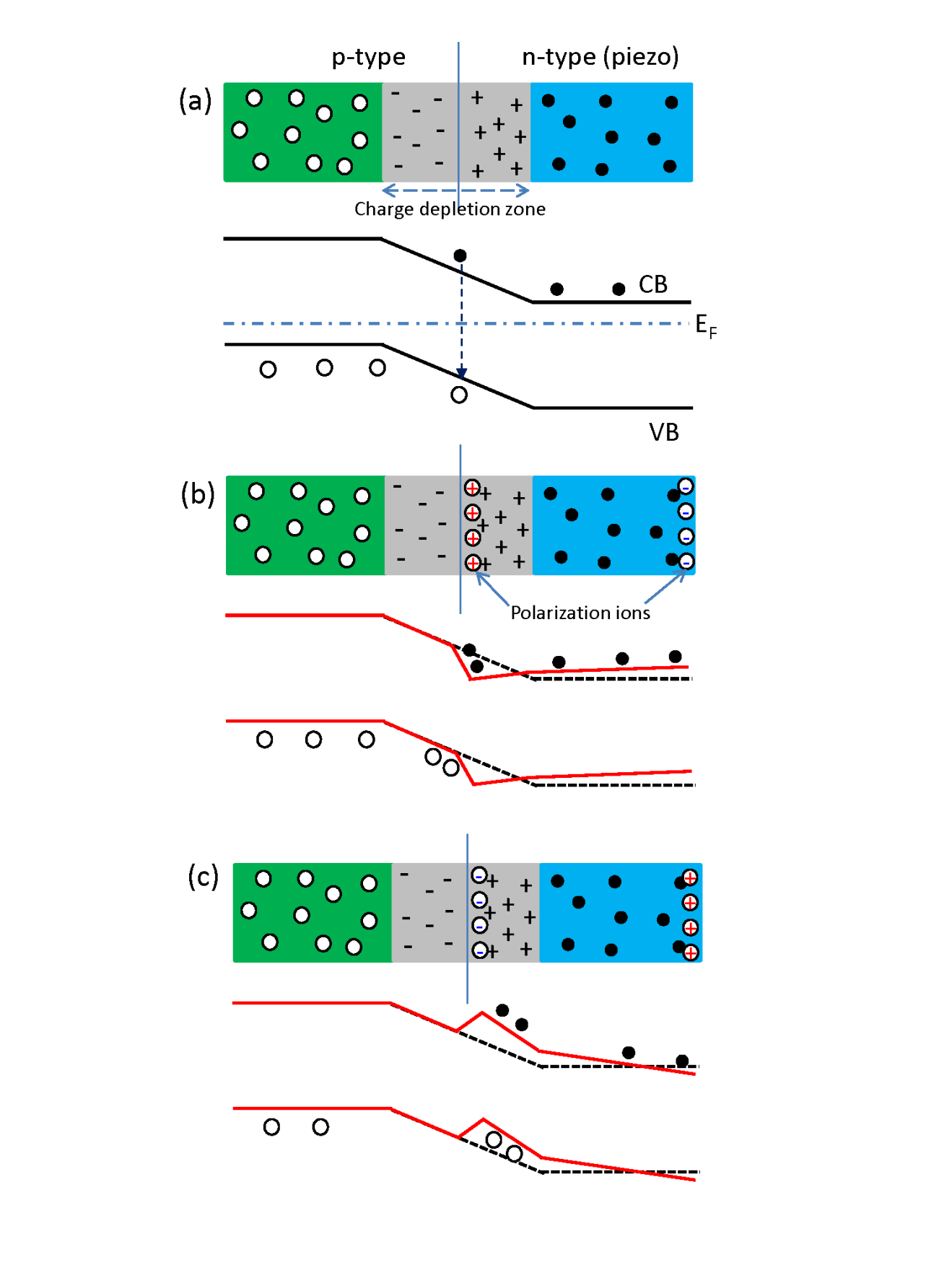
form a junction, the holes in the p-type side and the electrons in the n-type side tend to redistribute around the interface area to balance the local electric field
An electric field (sometimes E-field) is the physical field that surrounds electrically charged particles and exerts force on all other charged particles in the field, either attracting or repelling them. It also refers to the physical field fo ...
, which results in a charge depletion layer
In semiconductor physics, the depletion region, also called depletion layer, depletion zone, junction region, space charge region or space charge layer, is an insulating region within a conductive, doped semiconductor material where the mobile ...
. The diffusion and recombination of the electrons and holes in the junction region is closely related to the optoelectronic
Optoelectronics (or optronics) is the study and application of electronic devices and systems that find, detect and control light, usually considered a sub-field of photonics. In this context, ''light'' often includes invisible forms of radiatio ...
properties of the device, which is greatly affected by the local electric field distribution. The existence of the piezo-charges at the interface introduces three effects: a shift in local electronic band structure
In solid-state physics, the electronic band structure (or simply band structure) of a solid describes the range of energy levels that electrons may have within it, as well as the ranges of energy that they may not have (called ''band gaps'' or '' ...
due to the introduced local potential, a tilt of the electronic band structure
In solid-state physics, the electronic band structure (or simply band structure) of a solid describes the range of energy levels that electrons may have within it, as well as the ranges of energy that they may not have (called ''band gaps'' or '' ...
over the junction region for the polarization existing in the piezoelectric
Piezoelectricity (, ) is the electric charge that accumulates in certain solid materials—such as crystals, certain ceramics, and biological matter such as bone, DNA, and various proteins—in response to applied Stress (mechanics), mechanical s ...
semiconductor, and a change in the charge depletion layer
In semiconductor physics, the depletion region, also called depletion layer, depletion zone, junction region, space charge region or space charge layer, is an insulating region within a conductive, doped semiconductor material where the mobile ...
due to the redistribution of the local charge carriers to balance the local piezo-charges. The positive piezoelectric
Piezoelectricity (, ) is the electric charge that accumulates in certain solid materials—such as crystals, certain ceramics, and biological matter such as bone, DNA, and various proteins—in response to applied Stress (mechanics), mechanical s ...
charges at the junction lower the energy band and the negative piezoelectric
Piezoelectricity (, ) is the electric charge that accumulates in certain solid materials—such as crystals, certain ceramics, and biological matter such as bone, DNA, and various proteins—in response to applied Stress (mechanics), mechanical s ...
charges raise the energy band in n-type semiconductor
An extrinsic semiconductor is one that has been '' doped''; during manufacture of the semiconductor crystal a trace element or chemical called a doping agent has been incorporated chemically into the crystal, for the purpose of giving it different ...
region near the junction region. A modification in the local band by piezopotential may be effective for trapping charges so that the electron-hole recombination rate can be largely enhanced, which is very beneficial for improving the efficiency of a light-emitting diode
A light-emitting diode (LED) is a semiconductor device that emits light when current flows through it. Electrons in the semiconductor recombine with electron holes, releasing energy in the form of photons. The color of the light (cor ...
. Furthermore, the inclined band tends to change the mobility of the carriers moving toward the junction.
The materials for piezo-phototronics should have three basic properties: piezoelectricity, semiconductor property, and photon excitation property Typical materials are the wurtzite structures, such as ZnO, GaN
The word Gan or the initials GAN may refer to:
Places
*Gan, a component of Hebrew placenames literally meaning "garden"
China
* Gan River (Jiangxi)
* Gan River (Inner Mongolia),
* Gan County, in Jiangxi province
* Gansu, abbreviated ''Gā ...
and InN
Inns are generally establishments or buildings where travelers can seek lodging, and usually, food and drink. Inns are typically located in the country or along a highway; before the advent of motorized transportation they also provided accommo ...
. the three-way coupling among piezoelectricity, photoexcitation and semiconductor properties, which is the basis of piezotronics
Piezotronics effect is using the piezoelectric potential (piezopotential) created in materials with piezoelectricity as a “gate” voltage to tune/control the charge carrier transport properties for fabricating new devices. Neil A Downie showed h ...
(piezoelectricity-semiconductor coupling), piezophotonics (piezoelectric-photon excitation coupling), optoelectronics, and piezo-phototronics piezoelectricity-semiconductor-photoexcitation). The core of these coupling relies on the piezopotential created by the piezoelectric materials.
Experimental realization
Van der Waals heterostructures A two-dimensional semiconductor (also known as 2D semiconductor) is a type of natural semiconductor with thicknesses on the atomic scale. Geim and Novoselov et al. initiated the field in 2004 when they reported a new semiconducting material graphene ...
based on graphene and transition metal dichalcogenides :image:Cadmium sulfide.jpg, 220px, Cadmium sulfide, a prototypical metal chalcogenide, is used as a yellow pigment.
A chalcogenide is a chemical compound consisting of at least one chalcogen anion and at least one more electropositive element. Altho ...
(TMD) are promising for the realization of piezophototronic effect. It has been shown that the photo-response of graphene/MoS2 junction can be tuned by means of tensile stress
In continuum mechanics, stress is a physical quantity. It is a quantity that describes the magnitude of forces that cause deformation. Stress is defined as ''force per unit area''. When an object is pulled apart by a force it will cause elonga ...
manifesting piezophototronic effect in TMD devices.
References
{{reflist Condensed matter physics Electrical phenomena Energy harvesting