|
Tape-out
In electronics and photonics design, tape-out or tapeout is the final result of the design process for integrated circuits or printed circuit boards before they are sent for manufacturing. The tapeout is specifically the point at which the graphic for the photomask of the circuit is sent to the fabrication facility. History Historically, the term references the early days of printed circuit design, when the enlarged (for higher precision) "artwork" for the photomask was manually "taped out" using black line tape (commonly Bishop Graphics crepe) and also Rubylith sheets. In the post-war era of the 1940–50s, the techniques developed for rapid and low-cost circuit reproduction evolved to photographically replicated 2D manufacturing. The verb "to tapeout" was already widely used for the process and adopted for transistor fabrication, which evolved to full integrated-circuit approaches. Procedures involved The term ''tapeout'' currently is used to describe the creation of the ... [...More Info...] [...Related Items...] OR: [Wikipedia] [Google] [Baidu] |
Integrated Circuit Design
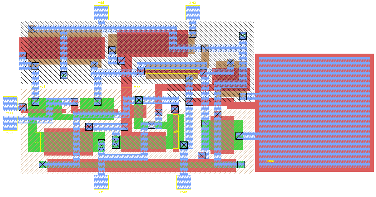
Integrated circuit design, or IC design, is a sub-field of electronics engineering, encompassing the particular logic and circuit design techniques required to design integrated circuits, or ICs. ICs consist of miniaturized electronic components built into an electrical network on a monolithic semiconductor substrate by photolithography. IC design can be divided into the broad categories of digital and analog IC design. Digital IC design is to produce components such as microprocessors, FPGAs, memories ( RAM, ROM, and flash) and digital ASICs. Digital design focuses on logical correctness, maximizing circuit density, and placing circuits so that clock and timing signals are routed efficiently. Analog IC design also has specializations in power IC design and RF IC design. Analog IC design is used in the design of op-amps, linear regulators, phase locked loops, oscillators and active filters. Analog design is more concerned with the physics of the semiconductor devices ... [...More Info...] [...Related Items...] OR: [Wikipedia] [Google] [Baidu] |
Integrated Circuit
An integrated circuit or monolithic integrated circuit (also referred to as an IC, a chip, or a microchip) is a set of electronic circuits on one small flat piece (or "chip") of semiconductor material, usually silicon. Transistor count, Large numbers of tiny MOSFETs (metal–oxide–semiconductor field-effect transistors) integrate into a small chip. This results in circuits that are orders of magnitude smaller, faster, and less expensive than those constructed of discrete electronic components. The IC's mass production capability, reliability, and building-block approach to integrated circuit design has ensured the rapid adoption of standardized ICs in place of designs using discrete transistors. ICs are now used in virtually all electronic equipment and have revolutionized the world of electronics. Computers, mobile phones and other home appliances are now inextricable parts of the structure of modern societies, made possible by the small size and low cost of ICs such as mode ... [...More Info...] [...Related Items...] OR: [Wikipedia] [Google] [Baidu] |
Signoff (electronic Design Automation)
In the automated design of integrated circuits, signoff (also written as sign-off) checks is the collective name given to a series of verification steps that the design must pass before it can be taped out. This implies an iterative process involving incremental fixes across the board using one or more check types, and then retesting the design. There are two types of sign-off's: front-end sign-off and back-end sign-off. After back-end sign-off the chip goes to fabrication. After listing out all the features in the specification, the verification engineer will write coverage for those features to identify bugs, and send back the RTL design to the designer. Bugs, or defects, can include issues like missing features (comparing the layout to the specification), errors in design (typo and functional errors), etc. When the coverage reaches a maximum% then the verification team will sign it off. By using a methodology like UVM, OVM, or VMM, the verification team develops a reusable envi ... [...More Info...] [...Related Items...] OR: [Wikipedia] [Google] [Baidu] |
Electronics Design
Electronic design automation (EDA), also referred to as electronic computer-aided design (ECAD), is a category of software tools for designing electronic systems such as integrated circuits and printed circuit boards. The tools work together in a design flow that chip designers use to design and analyze entire semiconductor chips. Since a modern semiconductor chip can have billions of components, EDA tools are essential for their design; this article in particular describes EDA specifically with respect to integrated circuits (ICs). History Early days Prior to the development of EDA, integrated circuits were designed by hand and manually laid out. Some advanced shops used geometric software to generate tapes for a Gerber photoplotter, responsible for generating a monochromatic exposure image, but even those copied digital recordings of mechanically drawn components. The process was fundamentally graphic, with the translation from electronics to graphics done manually; t ... [...More Info...] [...Related Items...] OR: [Wikipedia] [Google] [Baidu] |
Resolution Enhancement Technologies
Resolution(s) may refer to: Common meanings * Resolution (debate), the statement which is debated in policy debate * Resolution (law), a written motion adopted by a deliberative body * New Year's resolution, a commitment that an individual makes at New Year's Day * Dispute resolution, the settlement of a disagreement Science, technology, and mathematics Mathematics and logic * Resolution (algebra), an exact sequence in homological algebra * Resolution (logic), a rule of inference used for automated theorem proving * Standard resolution, the bar construction of resolutions in homological algebra * Resolution of singularities in algebraic geometry Measurements * Resolution (audio), a measure of digital audio quality * Resolution (electron density), the quality of an X-ray crystallography or cryo-electron microscopy data set * Angular resolution, the capability of an optical or other sensor to discern small objects * Depositional resolution, the age difference of f ... [...More Info...] [...Related Items...] OR: [Wikipedia] [Google] [Baidu] |
Semiconductor Fabrication
Semiconductor device fabrication is the process used to manufacture semiconductor devices, typically integrated circuit (IC) chips such as modern computer processors, microcontrollers, and memory chips such as NAND flash and DRAM that are present in everyday electrical and electronic devices. It is a multiple-step sequence of photolithographic and chemical processing steps (such as surface passivation, thermal oxidation, planar diffusion and junction isolation) during which electronic circuits are gradually created on a wafer made of pure semiconducting material. Silicon is almost always used, but various compound semiconductors are used for specialized applications. The entire manufacturing process takes time, from start to packaged chips ready for shipment, at least six to eight weeks (tape-out only, not including the circuit design) and is performed in highly specialized semiconductor fabrication plants, also called foundries or fabs. All fabrication takes place ... [...More Info...] [...Related Items...] OR: [Wikipedia] [Google] [Baidu] |
Prototype
A prototype is an early sample, model, or release of a product built to test a concept or process. It is a term used in a variety of contexts, including semantics, design, electronics, and software programming. A prototype is generally used to evaluate a new design to enhance precision by system analysts and users. Prototyping serves to provide specifications for a real, working system rather than a theoretical one. In some design workflow models, creating a prototype (a process sometimes called materialization) is the step between the formalization and the evaluation of an idea. A prototype can also mean a typical example of something such as in the use of the derivation 'prototypical'. This is a useful term in identifying objects, behaviours and concepts which are considered the accepted norm and is analogous with terms such as stereotypes and archetypes. The word ''prototype'' derives from the Greek , "primitive form", neutral of , "original, primitive", from πρ� ... [...More Info...] [...Related Items...] OR: [Wikipedia] [Google] [Baidu] |
Electronic Design Automation
Electronic design automation (EDA), also referred to as electronic computer-aided design (ECAD), is a category of software tools for designing electronic systems such as integrated circuits and printed circuit boards. The tools work together in a design flow that chip designers use to design and analyze entire semiconductor chips. Since a modern semiconductor chip can have billions of components, EDA tools are essential for their design; this article in particular describes EDA specifically with respect to integrated circuits (ICs). History Early days Prior to the development of EDA, integrated circuits were designed by hand and manually laid out. Some advanced shops used geometric software to generate tapes for a Gerber photoplotter, responsible for generating a monochromatic exposure image, but even those copied digital recordings of mechanically drawn components. The process was fundamentally graphic, with the translation from electronics to graphics done manually; t ... [...More Info...] [...Related Items...] OR: [Wikipedia] [Google] [Baidu] |
John Wawrzynek
John Wawrzynek is Professor of Electrical Engineering and Computer Science at the University of California at Berkeley. He holds a joint appointment with Lawrence Berkeley National Laboratory Lawrence Berkeley National Laboratory (LBNL), commonly referred to as the Berkeley Lab, is a United States national laboratory that is owned by, and conducts scientific research on behalf of, the United States Department of Energy. Located in ... and is the Chief Faculty Director of the Berkeley Wireless Research Center. He is currently a principal researcher in multiple large research centers at UC Berkeley including Algorithms and Specializers for Provably Optimal Implementations with Resilience and Efficiency (ASPIRE), the Parallel Computing Laboratory (ParLab), and the TerraSwarm Research Center.https://www.terraswarm.org / References External links John Wawrzynek's Berkeley EECS webpage {{DEFAULTSORT:Wawrzynek, John American computer scientists California Institute of Te ... [...More Info...] [...Related Items...] OR: [Wikipedia] [Google] [Baidu] |
Optical Proximity Correction
Optical proximity correction (OPC) is a photolithography enhancement technique commonly used to compensate for image errors due to diffraction or process effects. The need for OPC is seen mainly in the making of semiconductor devices and is due to the limitations of light to maintain the edge placement integrity of the original design, after processing, into the etched image on the silicon wafer. These projected images appear with irregularities such as line widths that are narrower or wider than designed, these are amenable to compensation by changing the pattern on the photomask used for imaging. Other distortions such as rounded corners are driven by the resolution of the optical imaging tool and are harder to compensate for. Such distortions, if not corrected for, may significantly alter the electrical properties of what was being fabricated. Optical proximity correction corrects these errors by moving edges or adding extra polygons to the pattern written on the photomask. This ... [...More Info...] [...Related Items...] OR: [Wikipedia] [Google] [Baidu] |
Mask Data Preparation
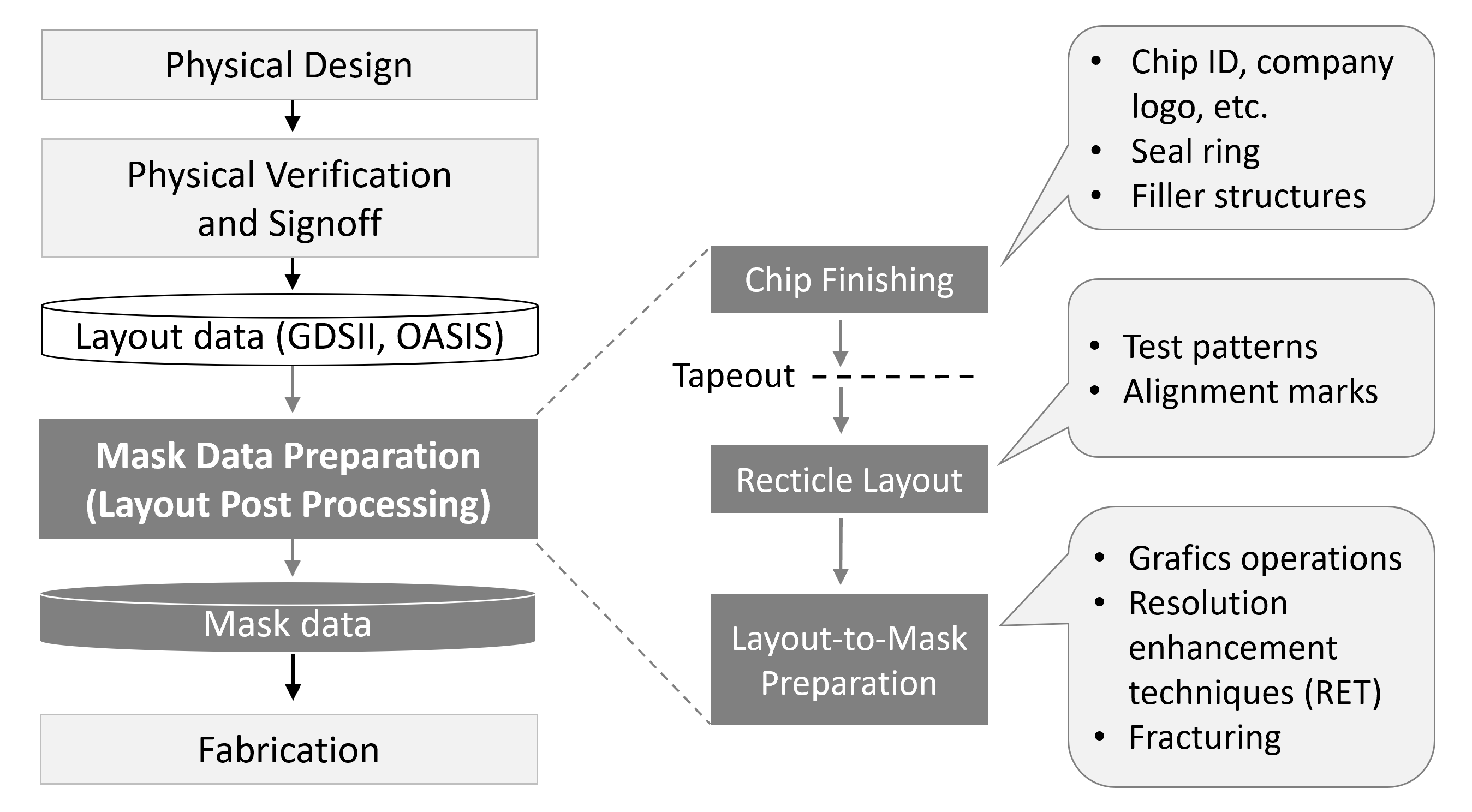
Mask data preparation (MDP), also known as layout post processing, is the procedure of translating a file containing the intended set of polygons from an integrated circuit layout into set of instructions that a photomask writer can use to generate a physical mask. Typically, amendments and additions to the chip layout are performed in order to convert the physical layout into data for mask production. Mask data preparation requires an input file which is in a GDSII or OASIS format, and produces a file that is in a proprietary format specific to the mask writer. MDP procedures Although historically converting the physical layout into data for mask production was relatively simple, more recent MDP procedures require various procedures: * ''Chip finishing'' which includes custom designations and structures to improve manufacturability of the layout. Examples of the latter are a seal ring and filler structures. * Producing a ''reticle layout'' with test patterns and alignme ... [...More Info...] [...Related Items...] OR: [Wikipedia] [Google] [Baidu] |
Design For Manufacturability (IC)
Design for manufacturability (also sometimes known as design for manufacturing or DFM) is the general engineering practice of designing products in such a way that they are easy to manufacture. The concept exists in almost all engineering disciplines, but the implementation differs widely depending on the manufacturing technology. DFM describes the process of designing or engineering a product in order to facilitate the manufacturing process in order to reduce its manufacturing costs. DFM will allow potential problems to be fixed in the design phase which is the least expensive place to address them. Other factors may affect the manufacturability such as the type of raw material, the form of the raw material, dimensional tolerances, and secondary processing such as finishing. Depending on various types of manufacturing processes there are set guidelines for DFM practices. These DFM guidelines help to precisely define various tolerances, rules and common manufacturing checks rela ... [...More Info...] [...Related Items...] OR: [Wikipedia] [Google] [Baidu] |

.jpg)


