|
Metal–nitride–oxide–semiconductor Transistor
The metal–nitride–oxide–semiconductor or metal–nitride–oxide–silicon (MNOS) transistor is a type of MOSFET (metal-oxide-semiconductor field-effect transistor) in which the oxide layer is replaced by a double layer of nitride and oxide. It is an alternative and supplement to the existing standard MOS technology, wherein the insulation employed is a nitride-oxide layer. It is used in non-volatile computer memory. History The original MOSFET (metal-oxide-semiconductor field-effect transistor, or MOS transistor) was invented by Egyptian engineer Mohamed M. Atalla and Korean engineer Dawon Kahng at Bell Labs in 1959, and demonstrated in 1960. Kahng went on to invent the floating-gate MOSFET with Simon Min Sze at Bell Labs, and they proposed its use as a floating-gate (FG) memory cell, in 1967. This was the first form of non-volatile memory based on the injection and storage of charges in a floating-gate MOSFET, which later became the basis for EPROM (erasable PROM), E ... [...More Info...] [...Related Items...] OR: [Wikipedia] [Google] [Baidu] |
MOSFET
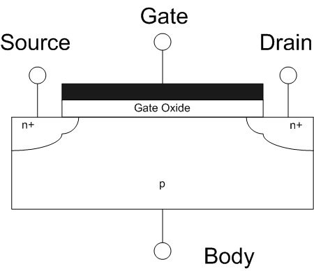
The metal–oxide–semiconductor field-effect transistor (MOSFET, MOS-FET, or MOS FET) is a type of field-effect transistor (FET), most commonly fabricated by the controlled oxidation of silicon. It has an insulated gate, the voltage of which determines the conductivity of the device. This ability to change conductivity with the amount of applied voltage can be used for amplifying or switching electronic signals. A metal-insulator-semiconductor field-effect transistor (MISFET) is a term almost synonymous with MOSFET. Another synonym is IGFET for insulated-gate field-effect transistor. The basic principle of the field-effect transistor was first patented by Julius Edgar Lilienfeld in 1925.Lilienfeld, Julius Edgar (1926-10-08) "Method and apparatus for controlling electric currents" upright=1.6, Two power MOSFETs in V_in_the_''off''_state,_and_can_conduct_a_continuous_current_of_30 surface-mount_packages._Operating_as_switches,_each_of_these_components_can_su ... [...More Info...] [...Related Items...] OR: [Wikipedia] [Google] [Baidu] |
Programmable Read-only Memory
A programmable read-only memory (PROM) is a form of digital memory where the contents can be changed once after manufacture of the device. The data is then permanent and cannot be changed. It is one type of read-only memory (ROM). PROMs are used in digital electronic devices to store permanent data, usually low level programs such as firmware or microcode. The key difference from a standard ROM is that the data is written into a ROM during manufacture, while with a PROM the data is programmed into them after manufacture. Thus, ROMs tend to be used only for large production runs with well-verified data. PROMs may be used where the volume required does not make a factory-programmed ROM economical, or during development of a system that may ultimately be converted to ROMs in a mass produced version. PROMs are manufactured blank and, depending on the technology, can be programmed at wafer, final test, or in system. Blank PROM chips are programmed by plugging them into a device ca ... [...More Info...] [...Related Items...] OR: [Wikipedia] [Google] [Baidu] |
Transistor Types
upright=1.4, gate (G), body (B), source (S) and drain (D) terminals. The gate is separated from the body by an insulating layer (pink). A transistor is a semiconductor device used to Electronic amplifier, amplify or electronic switch, switch electrical signals and electrical power, power. The transistor is one of the basic building blocks of modern electronics. It is composed of semiconductor material, usually with at least three terminals for connection to an electronic circuit. A voltage or current applied to one pair of the transistor's terminals controls the current through another pair of terminals. Because the controlled (output) power can be higher than the controlling (input) power, a transistor can amplify a signal. Some transistors are packaged individually, but many more are found embedded in integrated circuits. Austro-Hungarian physicist Julius Edgar Lilienfeld proposed the concept of a field-effect transistor in 1926, but it was not possible to actually const ... [...More Info...] [...Related Items...] OR: [Wikipedia] [Google] [Baidu] |
SONOS
SONOS, short for "silicon–oxide–nitride–oxide–silicon", more precisely, " polycrystalline silicon"—"silicon dioxide"—" silicon nitride"—"silicon dioxide"—"silicon", is a cross sectional structure of MOSFET (metal-oxide-semiconductor field-effect transistor), realized by P.C.Y. Chen of Fairchild Camera and Instrument in 1977. This structure is often used for non-volatile memories, such as EEPROM and flash memories. It is sometimes used for TFT LCD displays. It is one of CTF (charge trap flash) variants. It is distinguished from traditional non-volatile memory structures by the use of silicon nitride (Si3N4 or Si9N10) instead of "polysilicon-based FG (floating-gate)" for the charge storage material. A further variant is "SHINOS" ("silicon"—" hi-k"—"nitride"—"oxide"—"silicon"), which is substituted top oxide layer with high-κ material. Another advanced variant is "MONOS" ("metal–oxide–nitride–oxide–silicon"). Companies offering SONOS ... [...More Info...] [...Related Items...] OR: [Wikipedia] [Google] [Baidu] |
MISFET
The metal–oxide–semiconductor field-effect transistor (MOSFET, MOS-FET, or MOS FET) is a type of field-effect transistor (FET), most commonly fabricated by the controlled oxidation of silicon. It has an insulated gate, the voltage of which determines the conductivity of the device. This ability to change conductivity with the amount of applied voltage can be used for amplifying or switching electronic signals. A metal-insulator-semiconductor field-effect transistor (MISFET) is a term almost synonymous with MOSFET. Another synonym is IGFET for insulated-gate field-effect transistor. The basic principle of the field-effect transistor was first patented by Julius Edgar Lilienfeld in 1925.Lilienfeld, Julius Edgar (1926-10-08) "Method and apparatus for controlling electric currents" upright=1.6, Two power MOSFETs in V_in_the_''off''_state,_and_can_conduct_a_continuous_current_of_30 surface-mount_packages._Operating_as_switches,_each_of_these_components_can_su ... [...More Info...] [...Related Items...] OR: [Wikipedia] [Google] [Baidu] |
Field-effect Transistor
The field-effect transistor (FET) is a type of transistor that uses an electric field to control the flow of current in a semiconductor. FETs ( JFETs or MOSFETs) are devices with three terminals: ''source'', ''gate'', and ''drain''. FETs control the flow of current by the application of a voltage to the gate, which in turn alters the conductivity between the drain and source. FETs are also known as unipolar transistors since they involve single-carrier-type operation. That is, FETs use either electrons (n-channel) or holes (p-channel) as charge carriers in their operation, but not both. Many different types of field effect transistors exist. Field effect transistors generally display very high input impedance at low frequencies. The most widely used field-effect transistor is the MOSFET (metal-oxide-semiconductor field-effect transistor). History The concept of a field-effect transistor (FET) was first patented by Austro-Hungarian physicist Julius Edgar Lilienfeld in ... [...More Info...] [...Related Items...] OR: [Wikipedia] [Google] [Baidu] |
Silicon Nitride
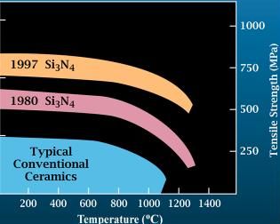
Silicon nitride is a chemical compound of the elements silicon and nitrogen. is the most thermodynamically stable and commercially important of the silicon nitrides, and the term "silicon nitride" commonly refers to this specific composition. It is a white, high-melting-point solid that is relatively chemically inert, being attacked by dilute HF and hot . It is very hard (8.5 on the mohs scale). It has a high thermal stability with strong optical nonlinearities for all-optical applications. Production Silicon nitride is prepared by heating powdered silicon between 1300 °C and 1400 °C in a nitrogen atmosphere: :3 Si + 2 → The silicon sample weight increases progressively due to the chemical combination of silicon and nitrogen. Without an iron catalyst, the reaction is complete after several hours (~7), when no further weight increase due to nitrogen absorption (per gram of silicon) is detected. In addition to , several other silicon nitride phases (with chemica ... [...More Info...] [...Related Items...] OR: [Wikipedia] [Google] [Baidu] |
Dielectric
In electromagnetism, a dielectric (or dielectric medium) is an electrical insulator that can be polarised by an applied electric field. When a dielectric material is placed in an electric field, electric charges do not flow through the material as they do in an electrical conductor, because they have no loosely bound, or free, electrons that may drift through the material, but instead they shift, only slightly, from their average equilibrium positions, causing dielectric polarisation. Because of dielectric polarisation, positive charges are displaced in the direction of the field and negative charges shift in the direction opposite to the field (for example, if the field is moving parallel to the positive ''x'' axis, the negative charges will shift in the negative ''x'' direction). This creates an internal electric field that reduces the overall field within the dielectric itself. If a dielectric is composed of weakly bonded molecules, those molecules not only become polaris ... [...More Info...] [...Related Items...] OR: [Wikipedia] [Google] [Baidu] |
Polysilicon
Polycrystalline silicon, or multicrystalline silicon, also called polysilicon, poly-Si, or mc-Si, is a high purity, polycrystalline form of silicon, used as a raw material by the solar photovoltaic and electronics industry. Polysilicon is produced from metallurgical grade silicon by a chemical purification process, called the Siemens process. This process involves distillation of volatile silicon compounds, and their decomposition into silicon at high temperatures. An emerging, alternative process of refinement uses a fluidized bed reactor. The photovoltaic industry also produces upgraded metallurgical-grade silicon (UMG-Si), using metallurgical instead of chemical purification processes. When produced for the electronics industry, polysilicon contains impurity levels of less than one part per billion (ppb), while polycrystalline solar grade silicon (SoG-Si) is generally less pure. A few companies from China, Germany, Japan, Korea and the United States, such as GCL-Poly, Wacker ... [...More Info...] [...Related Items...] OR: [Wikipedia] [Google] [Baidu] |
Charge Trap Flash
Charge trap flash (CTF) is a semiconductor memory technology used in creating non-volatile NOR and NAND flash memory. It is a type of floating-gate MOSFET memory technology, but differs from the conventional floating-gate technology in that it uses a silicon nitride film to store electrons rather than the doped polycrystalline silicon typical of a floating-gate structure. This approach allows memory manufacturers to reduce manufacturing costs five ways: # Fewer process steps are required to form a charge storage node # Smaller process geometries can be used (therefore reducing chip size and cost) # Multiple bits can be stored on a single flash memory cell # Improved reliability # Higher yield since the charge trap is less susceptible to point defects in the tunnel oxide layer While the charge-trapping concept was around earlier, it wasn't until 2002 that AMD and Fujitsu produced high-volume charge-trapping flash memory. They began the commercial production of charge-trapping flash ... [...More Info...] [...Related Items...] OR: [Wikipedia] [Google] [Baidu] |
Nitride
In chemistry, a nitride is an inorganic compound of nitrogen. The "nitride" anion, N3- ion, is very elusive but compounds of nitride are numerous, although rarely naturally occuring. Some nitrides have a find applications, such as wear-resistant coatings (e.g., titanium nitride, TiN), hard ceramic materials (e.g., silicon nitride, Si3N4), and semiconductors (e.g., gallium nitride, GaN). The development of GaN-based light emitting diodes was recognized by the 2014 Nobel Prize in Physics. Metal nitrido complexes are also common. Synthesis of inorganic metal nitrides is challenging because nitrogen gas (N2) is not very reactive at low temperatures, but it becomes more reactive at higher temperatures. Therefore, a balance must be achieved between the low reactivity of nitrogen gas at low temperatures and the entropy driven formation of N2 at high temperatures. However, synthetic methods for nitrides are growing more sophisticated and the materials are of increasing technological ... [...More Info...] [...Related Items...] OR: [Wikipedia] [Google] [Baidu] |
Sperry Corporation
Sperry Corporation was a major American equipment and electronics company whose existence spanned more than seven decades of the 20th century. Sperry ceased to exist in 1986 following a prolonged hostile takeover bid engineered by Burroughs Corporation, which merged the combined operation under the new name Unisys. Some of Sperry's former divisions became part of Honeywell, Lockheed Martin, Raytheon Technologies, and Northrop Grumman. The company is best known as the developer of the artificial horizon and a wide variety of other gyroscope-based aviation instruments like autopilots, bombsights, analog ballistics computers and gyro gunsights. In the post-WWII era the company branched out into electronics, both aviation related, and later, computers. History Early history The company was founded in 1910 by Elmer Ambrose Sperry, as the Sperry Gyroscope Company, to manufacture navigation equipment—chiefly his own inventions the marine gyrostabilizer and the gyr ... [...More Info...] [...Related Items...] OR: [Wikipedia] [Google] [Baidu] |

.jpg)


