|
Geometric Diode
Geometric diodes, also known as morphological diodes, use the shape of their structure and ballistic / quasi- ballistic electron transport to create diode behavior. Geometric diodes differ from all other forms of diodes because they do not rely on a depletion region or a potential barrier to create their diode behavior. Instead of a potential barrier, an asymmetry in the geometry of the material (that is on the order of the mean free path of the charge carrier) creates an asymmetry in forward vs reverse bias current (aka a diode). Creating a geometric diode Geometric diodes are formed from one continuous material (adding a caveat for 2D-electron gasses which are layered systems) that has an asymmetry in the structure on the order of the size of the charge carrier's mean free path (MFP). Typical room temperature MFPs range from single digit nanometers for metals up to tens or hundreds of nms for semiconductors, and even >1 micrometer in select systems. This means that to create ... [...More Info...] [...Related Items...] OR: [Wikipedia] [Google] [Baidu] |
Ballistic Conduction
In mesoscopic physics, ballistic conduction (ballistic transport) is the unimpeded flow (or transport) of charge carriers (usually electrons), or energy-carrying particles, over relatively long distances in a material. In general, the resistivity of a material exists because an electron, while moving inside a medium, is scattered by impurities, defects, thermal fluctuations of ions in a crystalline solid, or, generally, by any freely-moving atom/molecule composing a gas or liquid. Without scattering, electrons simply obey Newton's second law of motion at non-relativistic speeds. The mean free path of a particle can be described as the average length that the particle can travel freely, i.e., before a collision, which could change its momentum. The mean free path can be increased by reducing the number of impurities in a crystal or by lowering its temperature. Ballistic transport is observed when the mean free path of the particle is (much) longer than the dimension of the medium ... [...More Info...] [...Related Items...] OR: [Wikipedia] [Google] [Baidu] |
Farad
The farad (symbol: F) is the unit of electrical capacitance, the ability of a body to store an electrical charge, in the International System of Units (SI). It is named after the English physicist Michael Faraday (1791–1867). In SI base units 1 F = 1 kg−1⋅ m−2⋅ s4⋅ A2. Definition The capacitance of a capacitor is one farad when one coulomb of charge changes the potential between the plates by one volt. Equally, one farad can be described as the capacitance which stores a one-coulomb charge across a potential difference of one volt. The relationship between capacitance, charge, and potential difference is linear. For example, if the potential difference across a capacitor is halved, the quantity of charge stored by that capacitor will also be halved. For most applications, the farad is an impractically large unit of capacitance. Most electrical and electronic applications are covered by the following SI prefixes: *1 mF (millifarad, one thousandth ... [...More Info...] [...Related Items...] OR: [Wikipedia] [Google] [Baidu] |
Rectifier
A rectifier is an electrical device that converts alternating current (AC), which periodically reverses direction, to direct current (DC), which flows in only one direction. The reverse operation (converting DC to AC) is performed by an Power inverter, inverter. The process is known as ''rectification'', since it "straightens" the direction of current. Physically, rectifiers take a number of forms, including Vacuum tube#Diodes, vacuum tube diodes, wet chemical cells, mercury-arc valves, stacks of copper and selenium rectifier, selenium oxide plates, Diode#Semiconductor diodes, semiconductor diodes, silicon-controlled rectifiers and other silicon-based semiconductor switches. Historically, even synchronous electromechanical switches and motor-generator sets have been used. Early radio receivers, called crystal radios, used a "Cat's-whisker detector, cat's whisker" of fine wire pressing on a crystal of galena (lead sulfide) to serve as a point-contact rectifier or "crystal detec ... [...More Info...] [...Related Items...] OR: [Wikipedia] [Google] [Baidu] |
Semiconductor Diode
A diode is a two-terminal electronic component that conducts current primarily in one direction (asymmetric conductance); it has low (ideally zero) resistance in one direction, and high (ideally infinite) resistance in the other. A diode vacuum tube or thermionic diode is a vacuum tube with two electrodes, a heated cathode and a plate, in which electrons can flow in only one direction, from cathode to plate. A semiconductor diode, the most commonly used type today, is a crystalline piece of semiconductor material with a p–n junction connected to two electrical terminals. Semiconductor diodes were the first semiconductor electronic devices. The discovery of asymmetric electrical conduction across the contact between a crystalline mineral and a metal was made by German physicist Ferdinand Braun in 1874. Today, most diodes are made of silicon, but other semiconducting materials such as gallium arsenide and germanium are also used. Among many uses, diodes are found in rect ... [...More Info...] [...Related Items...] OR: [Wikipedia] [Google] [Baidu] |
Rectenna
A rectenna (''rec''tifying ant''enna'') is a special type of receiving antenna that is used for converting electromagnetic energy into direct current (DC) electricity. They are used in wireless power transmission systems that transmit power by radio waves. A simple rectenna element consists of a dipole antenna with an RF diode connected across the dipole elements. The diode rectifies the AC induced in the antenna by the microwaves, to produce DC power, which powers a load connected across the diode. Schottky diodes are usually used because they have the lowest voltage drop and highest speed and therefore have the lowest power losses due to conduction and switching. Large rectennas consist of an array of many power receiving elements such as dipole antennas. Power beaming applications The invention of the rectenna in the 1960s made long distance wireless power transmission feasible. The rectenna was invented in 1964 and patented in 1969 by US electrical engineer William ... [...More Info...] [...Related Items...] OR: [Wikipedia] [Google] [Baidu] |
Nanowire
A nanowire is a nanostructure in the form of a wire with the diameter of the order of a nanometre (10−9 metres). More generally, nanowires can be defined as structures that have a thickness or diameter constrained to tens of nanometers or less and an unconstrained length. At these scales, quantum mechanical effects are important—which coined the term "quantum wires". Many different types of nanowires exist, including superconducting (e.g. Yttrium barium copper oxide, YBCO), metallic (e.g. nickel, Ni, platinum, Pt, gold, Au, Ag), semiconducting (e.g. Silicon nanowire, silicon nanowires (SiNWs), indium phosphide, InP, gallium nitride, GaN) and insulating (e.g. Silicon dioxide, SiO2, Titanium dioxide, TiO2). Molecular nanowires are composed of repeating molecular units either organic (e.g. DNA) or inorganic (e.g. Mo6S9−xIx). Characteristics file:SnSe@SWCNT.jpg, upright=1.2, Crystalline 2×2-atom tin selenide nanowire grown inside a single-wall carbon nanotube (tube diamete ... [...More Info...] [...Related Items...] OR: [Wikipedia] [Google] [Baidu] |
Silicon
Silicon is a chemical element with the symbol Si and atomic number 14. It is a hard, brittle crystalline solid with a blue-grey metallic luster, and is a tetravalent metalloid and semiconductor. It is a member of group 14 in the periodic table: carbon is above it; and germanium, tin, lead, and flerovium are below it. It is relatively unreactive. Because of its high chemical affinity for oxygen, it was not until 1823 that Jöns Jakob Berzelius was first able to prepare it and characterize it in pure form. Its oxides form a family of anions known as silicates. Its melting and boiling points of 1414 °C and 3265 °C, respectively, are the second highest among all the metalloids and nonmetals, being surpassed only by boron. Silicon is the eighth most common element in the universe by mass, but very rarely occurs as the pure element in the Earth's crust. It is widely distributed in space in cosmic dusts, planetoids, and planets as various forms of silicon dioxide ( ... [...More Info...] [...Related Items...] OR: [Wikipedia] [Google] [Baidu] |
Graphene
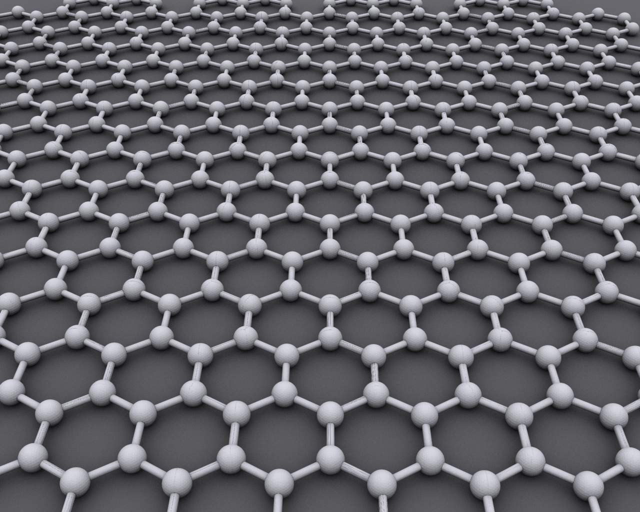
Graphene () is an allotrope of carbon consisting of a single layer of atoms arranged in a hexagonal lattice nanostructure. "Carbon nanostructures for electromagnetic shielding applications", Mohammed Arif Poothanari, Sabu Thomas, et al., ''Industrial Applications of Nanomaterials'', 2019. "Carbon nanostructures include various low-dimensional allotropes of carbon including carbon black (CB), carbon fiber, carbon nanotubes (CNTs), fullerene, and graphene." The name is derived from "graphite" and the suffix -ene, reflecting the fact that the allotrope of carbon contains numerous double bonds. Each atom in a graphene sheet is connecte ... [...More Info...] [...Related Items...] OR: [Wikipedia] [Google] [Baidu] |
Ratchet (device)
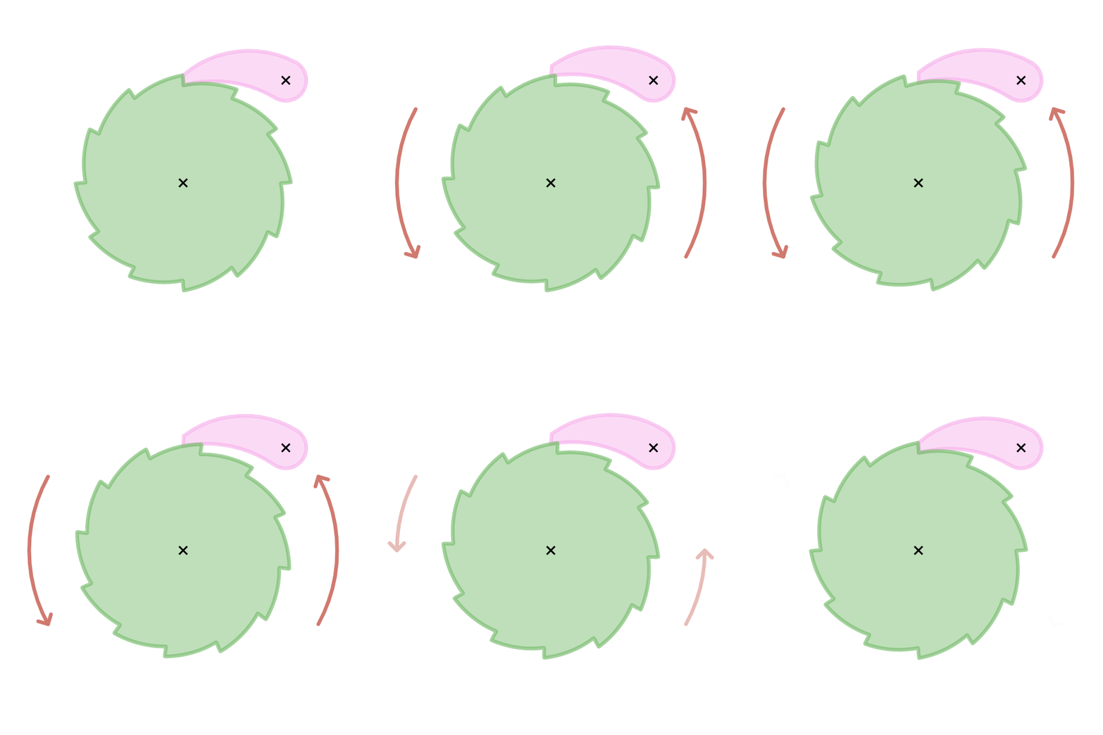
A ratchet (occasionally spelled rachet) is a mechanical device that allows continuous linear or rotary motion in only one direction while preventing motion in the opposite direction. Ratchets are widely used in machinery and tools. The word ''ratchet'' is also used informally to refer to a ratcheting socket wrench. __TOC__ Theory of operation A ratchet consists of a round gear or a linear rack with teeth, and a pivoting, spring-loaded finger called a '' pawl'' (or ''click'', in clocks and watches) that engages the teeth. The teeth are uniform but are usually asymmetrical, with each tooth having a moderate slope on one edge and a much steeper slope on the other edge. When the teeth are moving in the unrestricted (i.e. forward) direction, the pawl easily slides up and over the gently sloped edges of the teeth, with a spring forcing it (often with an audible 'click') into the depression between the teeth as it passes the tip of each tooth. When the teeth move in the opposite ... [...More Info...] [...Related Items...] OR: [Wikipedia] [Google] [Baidu] |
Photolithography
In integrated circuit manufacturing, photolithography or optical lithography is a general term used for techniques that use light to produce minutely patterned thin films of suitable materials over a substrate, such as a silicon wafer, to protect selected areas of it during subsequent etching, deposition, or implantation operations. Typically, ultraviolet light is used to transfer a geometric design from an optical mask to a light-sensitive chemical (photoresist) coated on the substrate. The photoresist either breaks down or hardens where it is exposed to light. The patterned film is then created by removing the softer parts of the coating with appropriate solvents. Conventional photoresists typically consists of three components: resin, sensitizer, and solvent. Photolithography processes can be classified according to the type of light used, such as ultraviolet, deep ultraviolet, extreme ultraviolet, or X-ray. The wavelength of light used determines the minimum feature si ... [...More Info...] [...Related Items...] OR: [Wikipedia] [Google] [Baidu] |
Nanolithography
Nanolithography (NL) is a growing field of techniques within nanotechnology dealing with the engineering (patterning e.g. etching, depositing, writing, printing etc) of nanometer-scale structures on various materials. The modern term reflects on a design of structures built in range of 10−9 to 10−6 meters, i.e. nanometer scale. Essentially, the field is a derivative of lithography, only covering very small structures. All NL methods can be categorized into four groups: photo lithography, scanning lithography, soft lithography and other miscellaneous techniques. History The NL has evolved from the need to increase the number of sub-micrometer features (e.g. transistors, capacitors etc.) in an integrated circuit in order to keep up with Moore's Law. While lithographic techniques have been around since the late 18th century, none were applied to nanoscale structures until the mid-1950s. With evolution of the semiconductor industry, demand for techniques capable of producing ... [...More Info...] [...Related Items...] OR: [Wikipedia] [Google] [Baidu] |
RC Time Constant
The RC time constant, also called tau, the time constant (in seconds) of an RC circuit, is equal to the product of the circuit resistance (in ohms) and the circuit capacitance (in farads), i.e. : \tau = RC econds It is the time required to charge the capacitor, through the resistor, from an initial charge voltage of zero to approximately 63.2% of the value of an applied DC voltage, or to discharge the capacitor through the same resistor to approximately 36.8% of its initial charge voltage. (These values are derived from the mathematical constant '' e'': 63.2\% \approx 1-e^ and 36.8\% \approx e^.) The following formulae use it, assuming a constant voltage applied across the capacitor and resistor in series, to determine the voltage across the capacitor against time: :Charging toward applied voltage (initially zero voltage across capacitor, constant across resistor and capacitor together) V_0: \quad V(t) = V_0(1-e^) :Discharging toward zero from initial voltage (initially ac ... [...More Info...] [...Related Items...] OR: [Wikipedia] [Google] [Baidu] |


