|
Fan-out Wafer-level Packaging
Fan-out wafer-level packaging (also known as wafer-level fan-out packaging, fan-out WLP, FOWL packaging, FO-WLP, FOWLP, etc.) is an integrated circuit packaging technology, and an enhancement of standard wafer-level packaging (WLP) solutions. In conventional technologies, a wafer is diced first, and then individual dies are packaged; package size is usually considerably larger than the die size. By contrast, in standard WLP flows integrated circuits are packaged while still part of the wafer, and the wafer (with outer layers of packaging already attached) is diced afterwards; the resulting package is practically of the same size as the die itself. However, the advantage of having a small package comes with a downside of limiting the number of external contacts that can be accommodated in the limited package footprint; this may become a significant limitation when complex semiconductor devices requiring a large number of contacts are considered. Fan-out WLP was developed to relax ... [...More Info...] [...Related Items...] OR: [Wikipedia] [Google] [Baidu] |
EWLB Sketch E
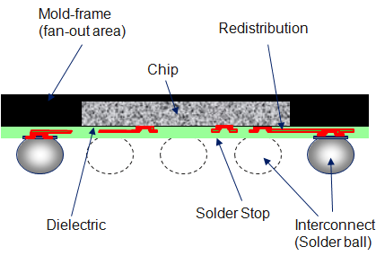
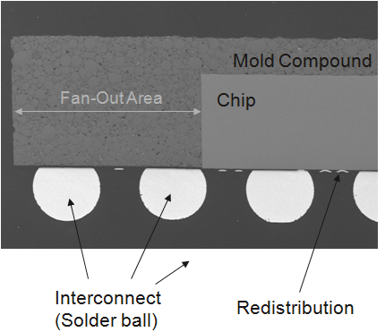
Embedded wafer level ball grid array (eWLB) is a packaging technology for integrated circuits. The package interconnects are applied on an artificial wafer made of silicon chips and a casting compound. eWLB is a further development of the classical wafer level ball grid array technology (WLB or WLP: wafer level package). The main driving force behind the eWLB technology was to allow fanout and more space for interconnect routing. All process steps for the generation of the package are performed on the wafer. This allows, in comparison to classical packaging technologies (e. g. ball grid array), the generation of very small and flat packages with excellent electrical and thermal performance at lowest cost. It is common for all WLB technologies, which are built on a silicon wafer, that the interconnects (typically solder balls) fit on the chip (so called fan-in design). Therefore only chips with a restricted number of interconnects can be packaged. The eWLB technology allows the ... [...More Info...] [...Related Items...] OR: [Wikipedia] [Google] [Baidu] |
Integrated Circuit Packaging
In electronics manufacturing, integrated circuit packaging is the final stage of semiconductor device fabrication, in which the block of semiconductor material is encapsulated in a supporting case that prevents physical damage and corrosion. The case, known as a " package", supports the electrical contacts which connect the device to a circuit board. In the integrated circuit industry, the process is often referred to as packaging. Other names include semiconductor device assembly, assembly, encapsulation or sealing. The packaging stage is followed by testing of the integrated circuit. The term is sometimes confused with electronic packaging, which is the mounting and interconnecting of integrated circuits (and other components) onto printed-circuit boards. Design considerations Electrical The current-carrying traces that run out of the die, through the package, and into the printed circuit board (PCB) have very different electrical properties compared to on-chip signal ... [...More Info...] [...Related Items...] OR: [Wikipedia] [Google] [Baidu] |
Wafer-level Packaging
Wafer-level packaging (WLP) is a process where packaging components are attached to an integrated circuit (IC) ''before'' the wafer – on which the IC is fabricated – is diced. In WSP, the top and bottom layers of the packaging and the solder bumps are attached to the integrated circuits while they are still in the wafer. This process differs from a conventional process, in which the wafer is sliced into individual circuits (dice) before the packaging components are attached. WLP is essentially a true chip-scale package (CSP) technology, since the resulting package is practically of the same size as the die. Wafer-level packaging allows integration of wafer fab, packaging, test, and burn-in at wafer level in order to streamline the manufacturing process undergone by a device from silicon start to customer shipment. There is no single industry-standard method of wafer-level packaging at present. A major application area of WLPs are smartphones due to the size constraints. For e ... [...More Info...] [...Related Items...] OR: [Wikipedia] [Google] [Baidu] |
Orbotech
Orbotech Ltd. a subsidiary of KLA Corporation and a technology company used in the manufacturing of consumer and industrial products throughout the electronics and adjacent industries. The company providing electronics reading, writing, and connecting solutions used by manufacturers of printed circuit boards, flat panel displays, advanced packaging, micro-electro-mechanical systems and other electronic components. The company is headquartered in Yavne, Israel and operates in North America, Europe, Japan and Asia-Pacific. Corporate history Early years Optrotech, one of the two companies which eventually merged to create Orbotech, was founded in 1981 by a team of engineers at Electro-Optical Industry Ltd. (El-Op) led by Shlomo Barak, who was developing electro-optical systems for military use, but saw commercial use for them as well. The company received financial backing from Uzia Galil of Elron Electronic Industries, an Israeli holding company. After 18 months of development, ... [...More Info...] [...Related Items...] OR: [Wikipedia] [Google] [Baidu] |
Wafer (electronics)
In electronics, a wafer (also called a slice or substrate) is a thin slice of semiconductor, such as a crystalline silicon Crystalline silicon or (c-Si) Is the crystalline forms of silicon, either polycrystalline silicon (poly-Si, consisting of small crystals), or monocrystalline silicon (mono-Si, a continuous crystal). Crystalline silicon is the dominant semiconduc ... (c-Si), used for the fabrication of integrated circuits and, in photovoltaics, to manufacture solar cells. The wafer serves as the substrate (materials science), substrate for microelectronic devices built in and upon the wafer. It undergoes many microfabrication processes, such as doping (semiconductor), doping, ion implantation, Etching (microfabrication), etching, thin-film deposition of various materials, and Photolithography, photolithographic patterning. Finally, the individual microcircuits are separated by wafer dicing and Integrated circuit packaging, packaged as an integrated circuit. History I ... [...More Info...] [...Related Items...] OR: [Wikipedia] [Google] [Baidu] |
Wafer Dicing
In the context of manufacturing integrated circuits, wafer dicing is the process by which die are separated from a wafer of semiconductor following the processing of the wafer. The dicing process can involve scribing and breaking, mechanical sawing (normally with a machine called a ''dicing saw'') or laser cutting. All methods are typically automated to ensure precision and accuracy. Following the dicing process the individual silicon chips are encapsulated into chip carriers which are then suitable for use in building electronic devices such as computers, etc. During dicing, wafers are typically mounted on dicing tape which has a sticky backing that holds the wafer on a thin sheet metal frame. Dicing tape has different properties depending on the dicing application. UV curable tapes are used for smaller sizes and non-UV dicing tape for larger die sizes. Dicing saws may use a dicing blade with diamond particles, rotating at 30,000 RPM and cooled with deionized water. Once a w ... [...More Info...] [...Related Items...] OR: [Wikipedia] [Google] [Baidu] |
Die (integrated Circuit)
A die, in the context of integrated circuits, is a small block of semiconducting material on which a given functional circuit is fabricated. Typically, integrated circuits are produced in large batches on a single wafer of electronic-grade silicon (EGS) or other semiconductor (such as GaAs) through processes such as photolithography. The wafer is cut (diced) into many pieces, each containing one copy of the circuit. Each of these pieces is called a die. There are three commonly used plural forms: ''dice'', ''dies'' and ''die''. To simplify handling and integration onto a printed circuit board, most dies are packaged in various forms. Manufacturing process Most dies are composed of silicon and used for integrated circuits. The process begins with the production of monocrystalline silicon ingots. These ingots are then sliced into disks with a diameter of up to 300 mm. [...More Info...] [...Related Items...] OR: [Wikipedia] [Google] [Baidu] |
Integrated Circuit
An integrated circuit or monolithic integrated circuit (also referred to as an IC, a chip, or a microchip) is a set of electronic circuits on one small flat piece (or "chip") of semiconductor material, usually silicon. Large numbers of tiny MOSFETs (metal–oxide–semiconductor field-effect transistors) integrate into a small chip. This results in circuits that are orders of magnitude smaller, faster, and less expensive than those constructed of discrete electronic components. The IC's mass production capability, reliability, and building-block approach to integrated circuit design has ensured the rapid adoption of standardized ICs in place of designs using discrete transistors. ICs are now used in virtually all electronic equipment and have revolutionized the world of electronics. Computers, mobile phones and other home appliances are now inextricable parts of the structure of modern societies, made possible by the small size and low cost of ICs such as modern computer ... [...More Info...] [...Related Items...] OR: [Wikipedia] [Google] [Baidu] |
Chip-scale Package
A chip scale package or chip-scale package (CSP) is a type of integrated circuit package. Originally, CSP was the acronym for ''chip-size packaging.'' Since only a few packages are chip size, the meaning of the acronym was adapted to ''chip-scale packaging''. According to IPC's standard J-STD-012, ''Implementation of Flip Chip and Chip Scale Technology'', in order to qualify as chip scale, the package must have an area no greater than 1.2 times that of the die and it must be a single-die, direct surface mountable package. Another criterion that is often applied to qualify these packages as CSPs is their ball pitch should be no more than 1 mm. The concept was first proposed by Junichi Kasai of Fujitsu and Gen Murakami of Hitachi Cable in 1993. The first concept demonstration however came from Mitsubishi Electric. The die may be mounted on an interposer upon which pads or balls are formed, like with flip chip ball grid array (BGA) packaging, or the pads may be etched or pr ... [...More Info...] [...Related Items...] OR: [Wikipedia] [Google] [Baidu] |
Fan-out
In digital electronics, the fan-out is the number of gate inputs driven by the output of another single logic gate. In most designs, logic gates are connected to form more complex circuits. While no logic gate input can be fed by more than one output at a time without causing contention, it is common for one output to be connected to several inputs. The technology used to implement logic gates usually allows a certain number of gate inputs to be wired directly together without additional interfacing circuitry. The maximum fan-out of an output measures its load-driving capability: it is the greatest number of inputs of gates of the same type to which the output can be safely connected. Logical practice Maximum limits on fan-out are usually stated for a given logic family or device in the manufacturer's datasheets. These limits assume that the driven devices are members of the same family. More complex analysis than fan-in and fan-out is required when two different logic fami ... [...More Info...] [...Related Items...] OR: [Wikipedia] [Google] [Baidu] |
Molding (process)
Molding (American English) or moulding (British and Commonwealth English; see spelling differences) is the process of manufacturing by shaping liquid or pliable raw material using a rigid frame called a mold or matrix. This itself may have been made using a pattern or model of the final object. A mold or mould is a hollowed-out block that is filled with a liquid or pliable material such as plastic, glass, metal, or ceramic raw material. The liquid hardens or sets inside the mold, adopting its shape. A mold is a counterpart to a cast. The very common bi-valve molding process uses two molds, one for each half of the object. Articulated molds have multiple pieces that come together to form the complete mold, and then disassemble to release the finished casting; they are expensive, but necessary when the casting shape has complex overhangs. Piece-molding uses a number of different molds, each creating a section of a complicated object. This is generally only used for larger a ... [...More Info...] [...Related Items...] OR: [Wikipedia] [Google] [Baidu] |
Redistribution Layer
A redistribution layer (RDL) is an extra metal layer on an integrated circuit that makes its IO pads available in other locations of the chip, for better access to the pads where necessary. When an integrated circuit is manufactured, it usually has a set of IO pads that are wirebonded to the pins of the package. A redistribution layer is an extra layer of wiring on the chip that enables bond out from different locations on the chip, making chip-to-chip bonding simpler. Another example of the use for RDL is for spreading the contact points around the die Die, as a verb, refers to death, the cessation of life. Die may also refer to: Games * Die, singular of dice, small throwable objects used for producing random numbers Manufacturing * Die (integrated circuit), a rectangular piece of a semicondu ... so that solder balls can be applied, and the thermal stress of mounting can be spread. References External links Redistribution tutorial Semiconductor device fabrication Pa ... [...More Info...] [...Related Items...] OR: [Wikipedia] [Google] [Baidu] |


.jpg)