|
Zinc Telluride
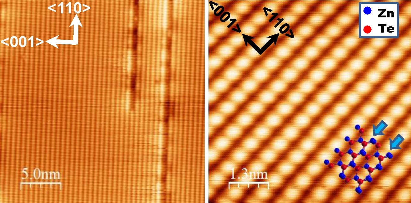
Zinc telluride is a binary chemical compound with the formula ZnTe. This solid is a semiconductor material with a direct band gap of 2.26 eV. It is usually a p-type semiconductor. Its crystal structure is cubic, like that for sphalerite and diamond. Properties ZnTe has the appearance of grey or brownish-red powder, or ruby-red crystals when refined by sublimation. Zinc telluride typically had a cubic (sphalerite, or " zincblende") crystal structure, but can be also prepared as rocksalt crystals or in hexagonal crystals ( wurtzite structure). Irradiated by a strong optical beam burns in presence of oxygen. Its lattice constant is 0.6101 nm, allowing it to be grown with or on aluminium antimonide, gallium antimonide, indium arsenide, and lead selenide. With some lattice mismatch, it can also be grown on other substrates such as GaAs, and it can be grown in thin-film polycrystalline (or nanocrystalline) form on substrates such as glass, for example, in the manufacture of ... [...More Info...] [...Related Items...] OR: [Wikipedia] [Google] [Baidu] |
Zincblende
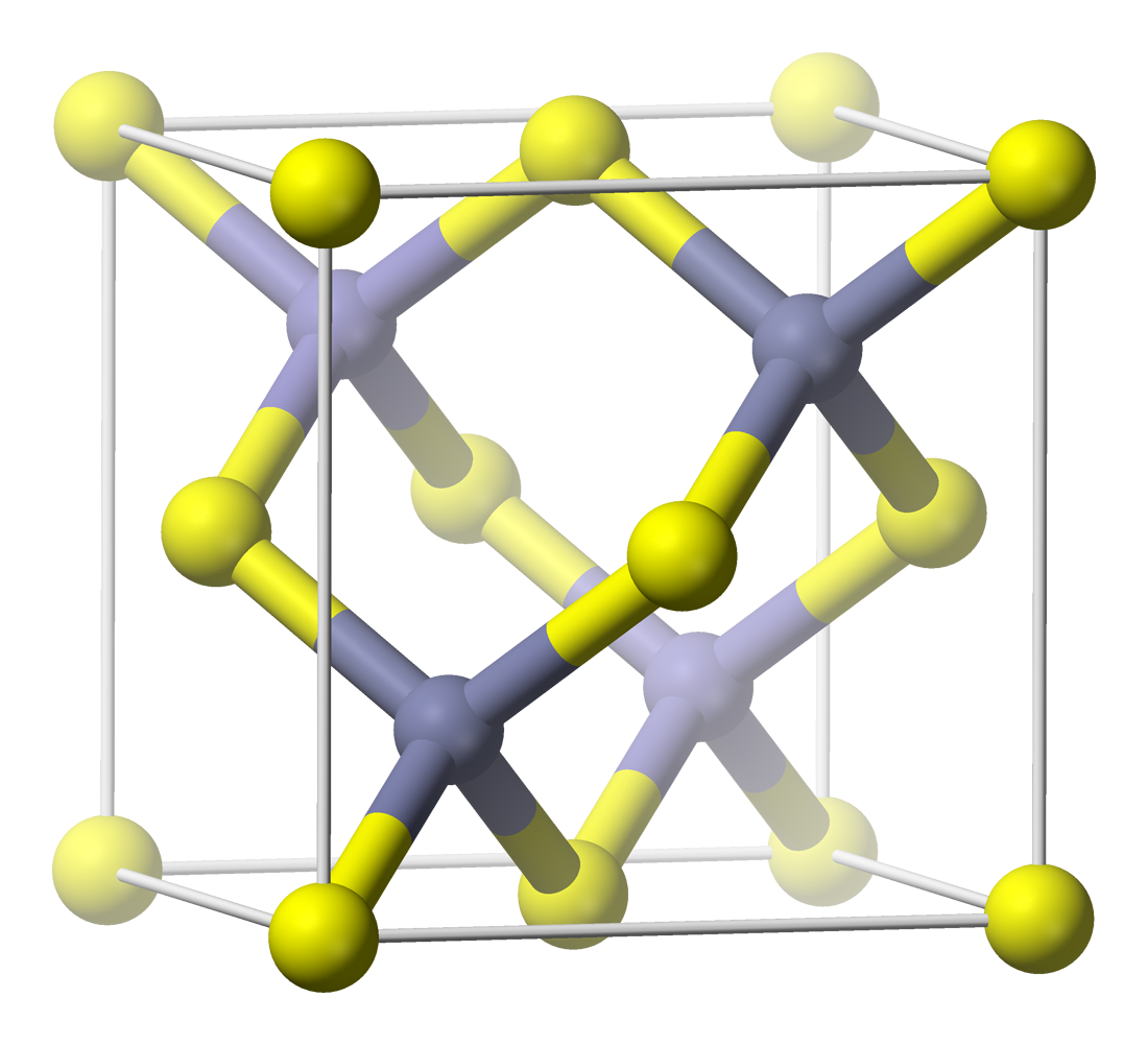
Sphalerite (sometimes spelled sphaelerite) is a sulfide mineral with the chemical formula . It is the most important ore of zinc. Sphalerite is found in a variety of deposit types, but it is primarily in sedimentary exhalative, Mississippi-Valley type, and volcanogenic massive sulfide deposits. It is found in association with galena, chalcopyrite, pyrite (and other sulfides), calcite, dolomite, quartz, rhodochrosite, and fluorite. German geologist Ernst Friedrich Glocker discovered sphalerite in 1847, naming it based on the Greek word ''sphaleros'', meaning "deceiving", due to the difficulty of identifying the mineral. In addition to zinc, sphalerite is an ore of cadmium, gallium, germanium, and indium. Miners have been known to refer to sphalerite as ''zinc blende'', ''black-jack'', and ''ruby blende''. Marmatite is an opaque black variety with a high iron content. Crystal habit and structure Sphalerite crystallizes in the face-centered cubic zincblende crystal structur ... [...More Info...] [...Related Items...] OR: [Wikipedia] [Google] [Baidu] |
Doping (semiconductor)
In semiconductor production, doping is the intentional introduction of impurities into an intrinsic semiconductor for the purpose of modulating its electrical, optical and structural properties. The doped material is referred to as an extrinsic semiconductor. Small numbers of dopant atoms can change the ability of a semiconductor to conduct electricity. When on the order of one dopant atom is added per 100 million atoms, the doping is said to be ''low'' or ''light''. When many more dopant atoms are added, on the order of one per ten thousand atoms, the doping is referred to as ''high'' or ''heavy''. This is often shown as ''n+'' for n-type doping or ''p+'' for p-type doping. (''See the article on semiconductors for a more detailed description of the doping mechanism.'') A semiconductor doped to such high levels that it acts more like a conductor than a semiconductor is referred to as a degenerate semiconductor. A semiconductor can be considered i-type semiconductor if it has ... [...More Info...] [...Related Items...] OR: [Wikipedia] [Google] [Baidu] |
Introduction To Solid State Physics
''Introduction to Solid State Physics'', known colloquially as ''Kittel'', is a classic condensed matter physics textbook written by American physicist Charles Kittel in 1953. The book has been highly influential and has seen widespread adoption; Marvin L. Cohen remarked in 2019 that Kittel's content choices in the original edition played a large role in defining the field of solid-state physics. It was also the first proper textbook covering this new field of physics. The book is published by John Wiley and Sons and, as of 2018, it is in its ninth edition and has been reprinted many times as well as translated into over a dozen languages, including Chinese, French, German, Hungarian, Indonesian, Italian, Japanese, Korean, Malay, Romanian, Russian, Spanish, and Turkish. In some later editions, the eighteenth chapter, titled ''Nanostructures'', was written by Paul McEuen. Along with its rival ''Ashcroft and Mermin'', the book is considered a standard textbook in condensed matter p ... [...More Info...] [...Related Items...] OR: [Wikipedia] [Google] [Baidu] |
Thin-film Solar Cells
A thin-film solar cell is a second generation solar cell that is made by depositing one or more thin layers, or thin film (TF) of photovoltaic material on a substrate, such as glass, plastic or metal. Thin-film solar cells are commercially used in several technologies, including cadmium telluride (CdTe), copper indium gallium diselenide (CIGS), and amorphous thin-film silicon (a-Si, TF-Si). Film thickness varies from a few nanometers ( nm) to tens of micrometers (µm), much thinner than thin-film's rival technology, the conventional, first-generation crystalline silicon solar cell (c-Si), that uses wafers of up to 200 µm thick. This allows thin film cells to be flexible, and lower in weight. It is used in building-integrated photovoltaics and as semi-transparent, photovoltaic glazing material that can be laminated onto windows. Other commercial applications use rigid thin film solar panels (interleaved between two panes of glass) in some of the world's largest photovolt ... [...More Info...] [...Related Items...] OR: [Wikipedia] [Google] [Baidu] |
Polycrystalline
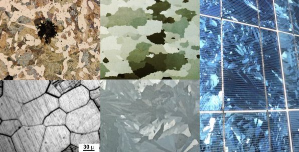
A crystallite is a small or even microscopic crystal which forms, for example, during the cooling of many materials. Crystallites are also referred to as grains. Bacillite is a type of crystallite. It is rodlike with parallel longulites. Structure The orientation of crystallites can be random with no preferred direction, called random texture, or directed, possibly due to growth and processing conditions. While the structure of a (single) crystal is highly ordered and its lattice is continuous and unbroken, amorphous materials, such as glass and many polymers, are non-crystalline and do not display any structures, as their constituents are not arranged in an ordered manner. Polycrystalline structures and paracrystalline phases are in-between these two extremes. Polycrystalline materials, or polycrystals, are solids that are composed of many crystallites of varying size and orientation. Most materials are polycrystalline, made of a large number crystallites held together by thi ... [...More Info...] [...Related Items...] OR: [Wikipedia] [Google] [Baidu] |
GaAs
Gallium arsenide (GaAs) is a III-V direct band gap semiconductor with a zinc blende crystal structure. Gallium arsenide is used in the manufacture of devices such as microwave frequency integrated circuits, monolithic microwave integrated circuits, infrared light-emitting diodes, laser diodes, solar cells and optical windows. GaAs is often used as a substrate material for the epitaxial growth of other III-V semiconductors, including indium gallium arsenide, aluminum gallium arsenide and others. Preparation and chemistry In the compound, gallium has a +3 oxidation state. Gallium arsenide single crystals can be prepared by three industrial processes: * The vertical gradient freeze (VGF) process. * Crystal growth using a horizontal zone furnace in the Bridgman-Stockbarger technique, in which gallium and arsenic vapors react, and free molecules deposit on a seed crystal at the cooler end of the furnace. * Liquid encapsulated Czochralski (LEC) growth is used for producing high-puri ... [...More Info...] [...Related Items...] OR: [Wikipedia] [Google] [Baidu] |
Lead Selenide
Lead selenide (PbSe), or lead(II) selenide, a selenide of lead, is a semiconductor material. It forms cubic crystals of the NaCl structure; it has a direct bandgap of 0.27 eV at room temperature. (Note that incorrectly identifies PbSe and other IV–VI semiconductors as indirect gap materials.) A grey solid, it is used for manufacture of infrared detectors for thermal imaging. The mineral clausthalite is a naturally occurring lead selenide. It may be formed by direct reaction between its constituent elements, lead and selenium. Infrared detection PbSe was one of the first materials found to be sensitive to the infrared radiation used for military applications. Early research works on the material as infrared detector were carried out during the 1930s and the first useful devices were processed by Germans, Americans and British during and just after World War II. Since then, PbSe has been commonly used as an infrared photodetector in multiple applications, from spectrome ... [...More Info...] [...Related Items...] OR: [Wikipedia] [Google] [Baidu] |
Indium Arsenide
Indium arsenide, InAs, or indium monoarsenide, is a narrow-bandgap semiconductor composed of indium and arsenic. It has the appearance of grey cubic crystals with a melting point of 942 °C. Indium arsenide is similar in properties to gallium arsenide and is a direct bandgap material, with a bandgap of 0.35 eV at room temperature. Indium arsenide is used for construction of infrared detectors, for the wavelength range of 1–3.8 µm. The detectors are usually photovoltaic photodiodes. Cryogenically cooled detectors have lower noise, but InAs detectors can be used in higher-power applications at room temperature as well. Indium arsenide is also used for making of diode lasers. InAs is well known for its high electron mobility and narrow energy bandgap. It is widely used as terahertz radiation source as it is a strong photo-Dember emitter. The optoelectronic properties and phonon vibrations are slightly changed under the effect of temperature over the range form 0 K ... [...More Info...] [...Related Items...] OR: [Wikipedia] [Google] [Baidu] |
Gallium Antimonide
Gallium antimonide (GaSb) is a semiconducting compound of gallium and antimony of the III-V family. It has a lattice constant of about 0.61 nm. It has a band gap of 0.67 eV. History The intermetallic compound GaSb was first prepared in 1926 by Victor Goldschmidt, who directly combined the elements under an inert gas atmosphere and reported on GaSb's lattice constant, which has since been revised. Goldschmidt also synthesized gallium phosphide and gallium arsenide. The Ga-Sb phase equilibria was investigated in 1955 by Koster and by Greenfield.Greenfield, I. G.; Smith, R. L., ''Trans. AIME'' 203, 351 (1955). Applications GaSb can be used for Infrared detectors, infrared LEDs and lasers and transistors, and thermophotovoltaic systems. See also * Aluminium antimonide * Indium antimonide * Gallium arsenide References External links properties listed at NSM Ioffe Institute. National Compound Semiconductor Roadmapat the Office of Naval Research The Office of Naval Research (ONR ... [...More Info...] [...Related Items...] OR: [Wikipedia] [Google] [Baidu] |
Aluminium Antimonide
Aluminium antimonide (AlSb) is a semiconductor of the group III-V family containing aluminium and antimony. The lattice constant is 0.61 nm. The indirect bandgap is approximately 1.6 electron volt, eV at 300 K, whereas the direct band gap is 2.22 eV. Its electron mobility is 200 cm²·V−1·s−1 and hole mobility 400 cm²·V−1·s−1 at 300 K. Its refractive index is 3.3 at a wavelength of 2 μm, and its dielectric constant is 10.9 at microwave frequencies.K Seeger and E Schonherr "Microwave dielectric constant of aluminium antimonide" Semicond. Sci. Technol. 6 (1991) 301 AlSb can be chemical reaction, reacted with other III-V materials to produce ternary materials including aluminium indium antimonide, AlInSb, AlGaSb and AlAsSb. Aluminum antimonide is rather flammable because of the reducing tendency of the antimonide (Sb3−) ion. It burns to produce aluminum oxide and antimony trioxide. See also * Gallium antimonide * Indium antimonide ... [...More Info...] [...Related Items...] OR: [Wikipedia] [Google] [Baidu] |
Lattice Constant
A lattice constant or lattice parameter is one of the physical dimensions and angles that determine the geometry of the unit cells in a crystal lattice, and is proportional to the distance between atoms in the crystal. A simple cubic crystal has only one lattice constant, the distance between atoms, but in general lattices in three dimensions have six lattice constants: the lengths ''a'', ''b'', and ''c'' of the three cell edges meeting at a vertex, and the angles ''α'', ''β'', and ''γ'' between those edges. The crystal lattice parameters ''a'', ''b'', and ''c'' have the dimension of length. The three numbers represent the size of the unit cell, that is, the distance from a given atom to an identical atom in the same position and orientation in a neighboring cell (except for very simple crystal structures, this will not necessarily be disance to the nearest neighbor). Their SI unit is the meter, and they are traditionally specified in angstroms (Å); an angstrom being 0.1 nanome ... [...More Info...] [...Related Items...] OR: [Wikipedia] [Google] [Baidu] |


