|
Tungsten Diselenide
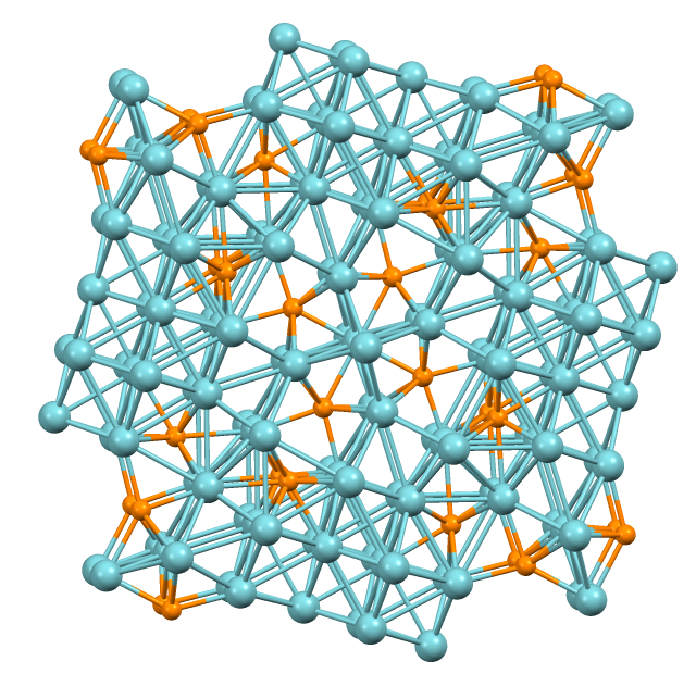
Tungsten diselenide is an inorganic compound with the formula WSe2. The compound adopts a hexagonal crystalline structure similar to molybdenum disulfide. Every tungsten atom is covalently bonded to six selenium ligands in a trigonal prismatic coordination sphere while each selenium is bonded to three tungsten atoms in a pyramidal geometry. The tungsten–selenium bond has a length of 0.2526 nm, and the distance between selenium atoms is 0.334 nm. It is a well studied example of a layered material. The layers stack together via van der Waals interactions. WSe2 is a very stable semiconductor in the group-VI transition metal dichalcogenides. Structure and properties The hexagonal (P63/mmc) polymorph 2H-WSe2 is isotypic with hexagonal MoS2. The two-dimensional lattice structure has W and Se arranged periodically in layers with hexagonal symmetry. Similar to graphite, van der Waals interactions hold the layers together; however, the 2D-layers in WSe2 are not atomicall ... [...More Info...] [...Related Items...] OR: [Wikipedia] [Google] [Baidu] |
Pearson Symbol
The Pearson symbol, or Pearson notation, is used in crystallography as a means of describing a crystal structure, and was originated by W. B. Pearson. The symbol is made up of two letters followed by a number. For example: * Diamond structure, ''cF''8 * Rutile structure, ''tP''6 The two (italicised) letters specify the Bravais lattice. The lower-case letter specifies the crystal family, and the upper-case letter the centering type. The number at the end of the Pearson symbol gives the number of the atoms in the conventional unit cell.Nomenclature of Inorganic Chemistry IUPAC Recommendations 2005 IR-3.4.4, pp. 49–51; IR-11.5, pp. 241–242. |
Sputter Deposition
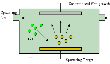
Sputter deposition is a physical vapor deposition (PVD) method of thin film deposition by the phenomenon of sputtering. This involves ejecting material from a "target" that is a source onto a "substrate" such as a silicon wafer. Resputtering is re-emission of the deposited material during the deposition process by ion or atom bombardment. Sputtered atoms ejected from the target have a wide energy distribution, typically up to tens of eV (100,000 K). The sputtered ions (typically only a small fraction of the ejected particles are ionized — on the order of 1 percent) can ballistically fly from the target in straight lines and impact energetically on the substrates or vacuum chamber (causing resputtering). Alternatively, at higher gas pressures, the ions collide with the gas atoms that act as a moderator and move diffusively, reaching the substrates or vacuum chamber wall and condensing after undergoing a random walk. The entire range from high-energy ballistic impact to low-energy ... [...More Info...] [...Related Items...] OR: [Wikipedia] [Google] [Baidu] |
Selenides
A selenide is a chemical compound containing a selenium anion with oxidation number of −2 (Se2−), much as sulfur does in a sulfide. The chemistry of the selenides and sulfides is similar. Similar to sulfide, in aqueous solution, the selenide ion, Se2−, is prevalent only in very basic conditions. In neutral conditions, hydrogen selenide ion, HSe−, is most common. In acid conditions, hydrogen selenide, H2Se, is formed. Some selenides are reactive to oxidation by air. Owing to the greater reducing power of selenide, metal selenides are more easily decomposed to the elements than are sulfides (tellurides are even more labile). Selenides of electropositive metals: such as aluminium selenide readily hydrolyse, even in moist air, evolving toxic hydrogen selenide gas. Pure selenide minerals are rare, instead selenium tends to partially substitute for sulfide in many sulfide minerals. The degree of substitution is only of commercial interest for copper sulfide ores, in which case ... [...More Info...] [...Related Items...] OR: [Wikipedia] [Google] [Baidu] |
Tungsten Compounds
Tungsten, or wolfram, is a chemical element with the symbol W and atomic number 74. Tungsten is a rare metal found naturally on Earth almost exclusively as compounds with other elements. It was identified as a new element in 1781 and first isolated as a metal in 1783. Its important ores include scheelite and wolframite, the latter lending the element its alternate name. The free element is remarkable for its robustness, especially the fact that it has the highest melting point of all known elements barring carbon (which sublimes at normal pressure), melting at . It also has the highest boiling point, at . Its density is , comparable with that of uranium and gold, and much higher (about 1.7 times) than that of lead. Polycrystalline tungsten is an intrinsically brittle and hard material (under standard conditions, when uncombined), making it difficult to work. However, pure single-crystalline tungsten is more ductile and can be cut with a hard-steel hacksaw. Tungsten occurs in many ... [...More Info...] [...Related Items...] OR: [Wikipedia] [Google] [Baidu] |
Light-emitting Diode
A light-emitting diode (LED) is a semiconductor device that emits light when current flows through it. Electrons in the semiconductor recombine with electron holes, releasing energy in the form of photons. The color of the light (corresponding to the energy of the photons) is determined by the energy required for electrons to cross the band gap of the semiconductor. White light is obtained by using multiple semiconductors or a layer of light-emitting phosphor on the semiconductor device. Appearing as practical electronic components in 1962, the earliest LEDs emitted low-intensity infrared (IR) light. Infrared LEDs are used in remote-control circuits, such as those used with a wide variety of consumer electronics. The first visible-light LEDs were of low intensity and limited to red. Early LEDs were often used as indicator lamps, replacing small incandescent bulbs, and in seven-segment displays. Later developments produced LEDs available in visible, ultraviolet (UV) ... [...More Info...] [...Related Items...] OR: [Wikipedia] [Google] [Baidu] |
Photovoltaics
Photovoltaics (PV) is the conversion of light into electricity using semiconducting materials that exhibit the photovoltaic effect, a phenomenon studied in physics, photochemistry, and electrochemistry. The photovoltaic effect is commercially used for electricity generation and as photosensors. A photovoltaic system employs solar modules, each comprising a number of solar cells, which generate electrical power. PV installations may be ground-mounted, rooftop-mounted, wall-mounted or floating. The mount may be fixed or use a solar tracker to follow the sun across the sky. Photovoltaic technology helps to mitigate climate change because it emits much less carbon dioxide than fossil fuels. Solar PV has specific advantages as an energy source: once installed, its operation generates no pollution and no greenhouse gas emissions, it shows scalability in respect of power needs and silicon has large availability in the Earth's crust, although other materials required in PV system m ... [...More Info...] [...Related Items...] OR: [Wikipedia] [Google] [Baidu] |
Graphene
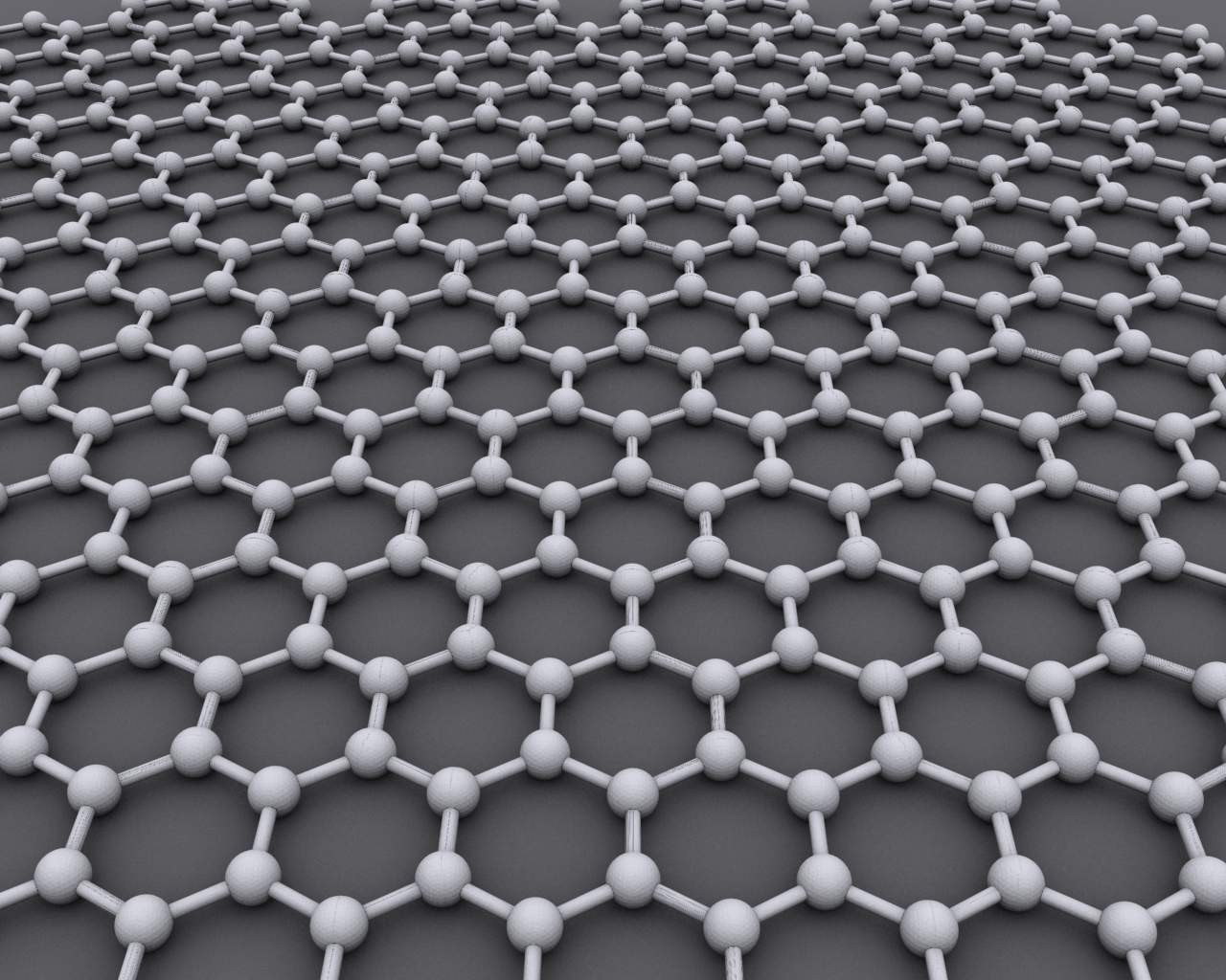
Graphene () is an allotrope of carbon consisting of a single layer of atoms arranged in a hexagonal lattice nanostructure. "Carbon nanostructures for electromagnetic shielding applications", Mohammed Arif Poothanari, Sabu Thomas, et al., ''Industrial Applications of Nanomaterials'', 2019. "Carbon nanostructures include various low-dimensional allotropes of carbon including carbon black (CB), carbon fiber, carbon nanotubes (CNTs), fullerene, and graphene." The name is derived from "graphite" and the suffix -ene, reflecting the fact that the allotrope of carbon contains numerous double bonds. Each atom in a graphene sheet is connecte ... [...More Info...] [...Related Items...] OR: [Wikipedia] [Google] [Baidu] |
Photoelectrochemical Cell
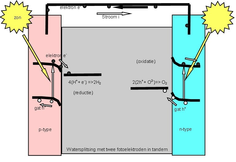
A "photoelectrochemical cell" is one of two distinct classes of device. The first produces electrical energy similarly to a dye-sensitized photovoltaic cell, which meets the standard definition of a photovoltaic cell. The second is a photoelectrolytic cell, that is, a device which uses light incident on a photosensitizer, semiconductor, or aqueous metal immersed in an electrolytic solution to directly cause a chemical reaction, for example to produce hydrogen via the electrolysis of water. Both types of device are varieties of solar cell, in that a photoelectrochemical cell's function is to use the photoelectric effect (or, very similarly, the photovoltaic effect) to convert electromagnetic radiation (typically sunlight) either directly into electrical power, or into something which can itself be easily used to produce electrical power (hydrogen, for example, can be burned to create electrical power, see photohydrogen). Two principles The standard photovoltaic effect, as ... [...More Info...] [...Related Items...] OR: [Wikipedia] [Google] [Baidu] |
Solar Cell
A solar cell, or photovoltaic cell, is an electronic device that converts the energy of light directly into electricity by the photovoltaic effect, which is a physical and chemical phenomenon.Solar Cells chemistryexplained.com It is a form of photoelectric cell, defined as a device whose electrical characteristics, such as , , or resistance, vary when exposed to light. Individual solar cell devices are often the electrical ... [...More Info...] [...Related Items...] OR: [Wikipedia] [Google] [Baidu] |
Dichalcogenide
: 220px, Cadmium sulfide, a prototypical metal chalcogenide, is used as a yellow pigment. A chalcogenide is a chemical compound consisting of at least one chalcogen anion and at least one more electropositive element. Although all group 16 elements of the periodic table are defined as chalcogens, the term chalcogenide is more commonly reserved for sulfides, selenides, tellurides, and polonides, rather than oxides. Many metal ores exist as chalcogenides. Photoconductive chalcogenide glasses are used in xerography. Some pigments and catalysts are also based on chalcogenides. The metal dichalcogenide MoS2 is a common solid lubricant. Alkali metal and alkaline earth chalcogenides Alkali metal and alkaline earth monochalcogenides are salt-like, being colourless and often water-soluble. The sulfides tend to undergo hydrolysis to form derivatives containing bisulfide (SH−) anions. The alkali metal chalcogenides often crystallize with the antifluorite structure and the alkaline earth s ... [...More Info...] [...Related Items...] OR: [Wikipedia] [Google] [Baidu] |
Transition Metal
In chemistry, a transition metal (or transition element) is a chemical element in the d-block of the periodic table (groups 3 to 12), though the elements of group 12 (and less often group 3) are sometimes excluded. They are the elements that can use d orbitals as valence orbitals to form chemical bonds. The lanthanide and actinide elements (the f-block) are called inner transition metals and are sometimes considered to be transition metals as well. Since they are metals, they are lustrous and have good electrical and thermal conductivity. Most (with the exception of group 11 and group 12) are hard and strong, and have high melting and boiling temperatures. They form compounds in any of two or more different oxidation states and bind to a variety of ligands to form coordination complexes that are often coloured. They form many useful alloys and are often employed as catalysts in elemental form or in compounds such as coordination complexes and oxides. Most are strongly param ... [...More Info...] [...Related Items...] OR: [Wikipedia] [Google] [Baidu] |


