|
Socket C32
Socket C32 is a zero insertion force land grid array CPU socket designed by AMD for their single-CPU and dual-CPU Opteron 4000 series server CPUs. It is the successor to Socket AM3 for single-CPU servers and the successor for Socket F for lower-end dual-CPU servers (High-end dual-CPU servers will use Socket G34). Socket C32 supports two DDR3 SDRAM channels. It is based on the Socket F and uses a similar 1207-pin LGA socket but is not physically or electrically compatible with Socket F due to the use of DDR3 SDRAM instead of the DDR2 SDRAM that Socket F platforms use. Socket C32 was launched on June 23, 2010 as part of the San Marino platform with the four and six-core Opteron 4100 "Lisbon" processors. Socket C32 also supports the Bulldozer-based six- and eight-core "Valencia" Opterons introduced in November 2011. Both Socket C32 and its contemporary Socket G34 were succeeded in 2017 by Socket SP3 for both single- and dual-CPU servers, supporting Zen-based Epyc CPUs, the suc ... [...More Info...] [...Related Items...] OR: [Wikipedia] [Google] [Baidu] |
Supermicro Dual Opteron Server Board Cpu Socket IMGP7338 Wp
Super Micro Computer, Inc., dba Supermicro, is an information technology company based in San Jose, California. It has manufacturing operations in the Silicon Valley, the Netherlands and at its Science and Technology Park in Taiwan. Founded on November 1, 1993, Supermicro is a provider of high-performance and high-efficiency servers, server management softwares, and storage systems for various markets, including enterprise data centers, cloud computing, artificial intelligence, 5G and edge computing. Supermicro’s stock trades under the ticker symbol SMCI on the Nasdaq exchange. Supermicro fiscal year 2022 revenues were $5.2 billion and Supermicro has 4,607 employees globally. History Formation and initial public offering In 1993, Supermicro began as a 5 person operation run by Charles Liang alongside his wife and company treasurer, Chiu-Chu Liu, known as Sara. In 1996, the company opened a manufacturing subsidiary in Taiwan, Ablecom, which is run by Charles’s broth ... [...More Info...] [...Related Items...] OR: [Wikipedia] [Google] [Baidu] |
Land Grid Array
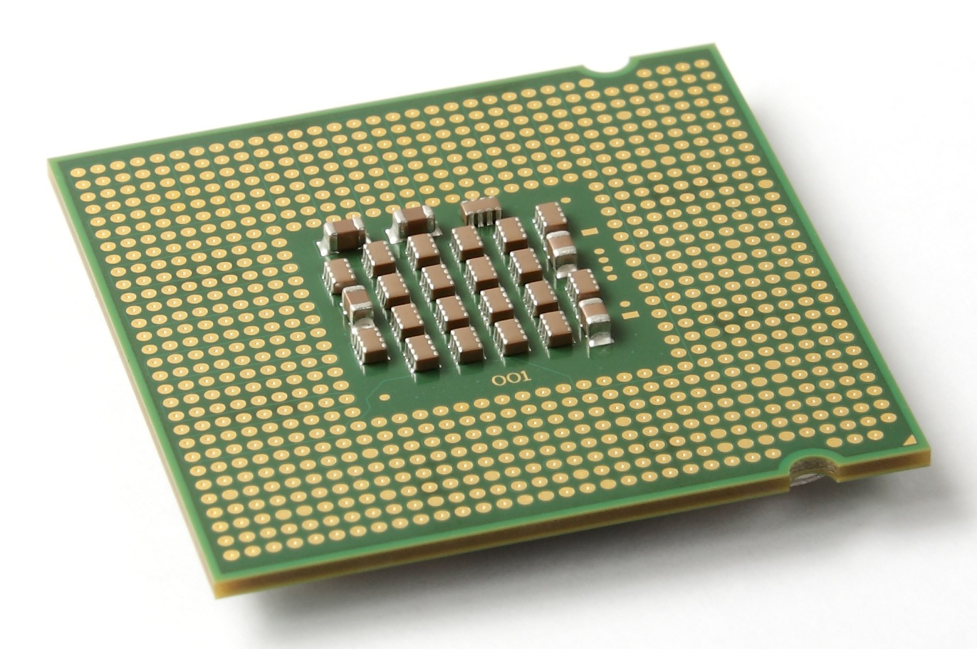
The land grid array (LGA) is a type of surface-mount packaging for integrated circuits (ICs) that is notable for having the pins on the socket (when a socket is used) rather than the integrated circuit. An LGA can be electrically connected to a printed circuit board (PCB) either by the use of a socket or by soldering directly to the board. Description The ''land grid array'' is a packaging technology with a grid of contacts, 'lands', on the underside of a package. The contacts are to be connected to a grid of contacts on the PCB. Not all rows and columns of the grid need to be used. The contacts can either be made by using an LGA socket, or by using solder paste. The grid elements found in use can be e.g. circular, triangular or other polygonal shapes and might have even different sizes. Grids might sometimes appear like honey comb patterns. Designs are often optimized for factors like contact likeliness despite tolerances, electrical gap to neighboring contacts and for allowin ... [...More Info...] [...Related Items...] OR: [Wikipedia] [Google] [Baidu] |
Epyc
Epyc is a brand of multi-core x86-64 microprocessors designed and sold by AMD, based on the company's Zen microarchitecture. Introduced in June 2017, they are specifically targeted for the server and embedded system markets. Epyc processors share the same microarchitecture as their regular desktop-grade counterparts, but have enterprise-grade features such as higher core counts, more PCI Express lanes, support for larger amounts of RAM, and larger cache memory. They also support multi-chip and dual-socket system configurations by using the Infinity Fabric interconnect. History In March 2017, AMD announced plans to re-enter the server market with a platform based on the Zen microarchitecture, codenamed Naples, and officially revealed it under the brand name Epyc in May. That June, AMD officially launched Epyc 7001 series processors, offering up to 32 cores per socket, and enabling performance that allowed Epyc to be competitive with the competing Intel Xeon product line. Two years ... [...More Info...] [...Related Items...] OR: [Wikipedia] [Google] [Baidu] |
Zen (microarchitecture)
Zen is the codename for a family of computer processor microarchitectures from AMD, first launched in February 2017 with the first generation of its Ryzen CPUs. It is used in Ryzen (desktop and mobile), Ryzen Threadripper (workstation/high end desktop), and Epyc (server). Comparison History First generation The first generation Zen was launched with the Ryzen 1000 series of CPUs (codenamed Summit Ridge) in February 2017. The first Zen-based preview system was demonstrated at E3 2016, and first substantially detailed at an event hosted a block away from the Intel Developer Forum 2016. The first Zen-based CPUs reached the market in early March 2017, and Zen-derived Epyc server processors (codenamed "Naples") launched in June 2017 and Zen-based APUs (codenamed "Raven Ridge") arrived in November 2017. This first iteration of Zen utilized Global Foundries' 14 nm manufacturing process. First generation refresh Zen+ was first released in April 2018, powering the second ... [...More Info...] [...Related Items...] OR: [Wikipedia] [Google] [Baidu] |
Bulldozer (processor)
The AMD Bulldozer Family 15h is a microprocessor microarchitecture for the FX and Opteron line of processors, developed by AMD for the desktop and server markets. Bulldozer is the codename for this family of microarchitectures. It was released on October 12, 2011, as the successor to the K10 microarchitecture. Bulldozer is designed from scratch, not a development of earlier processors. The core is specifically aimed at computing products with TDPs of 10 to 125 watts. AMD claims dramatic performance-per-watt efficiency improvements in high-performance computing (HPC) applications with Bulldozer cores. The ''Bulldozer'' cores support most of the instruction sets implemented by Intel processors (Sandy Bridge) available at its introduction (including SSE4.1, SSE4.2, AES, CLMUL, and AVX) as well as new instruction sets proposed by AMD; ABM, XOP, FMA4 and F16C. Only Bulldozer GEN4 (Excavator) supports AVX2 instruction sets. Overview According to AMD, Bulldozer-based CPUs ... [...More Info...] [...Related Items...] OR: [Wikipedia] [Google] [Baidu] |
DDR2 SDRAM
Double Data Rate 2 Synchronous Dynamic Random-Access Memory (DDR2 SDRAM) is a double data rate (DDR) synchronous dynamic random-access memory (SDRAM) interface. It superseded the original DDR SDRAM specification, and was itself superseded by DDR3 SDRAM (launched in 2007). DDR2 DIMMs are neither forward compatible with DDR3 nor backward compatible with DDR. In addition to double pumping the data bus as in DDR SDRAM (transferring data on the rising and falling edges of the bus clock signal), DDR2 allows higher bus speed and requires lower power by running the internal clock at half the speed of the data bus. The two factors combine to produce a total of four data transfers per internal clock cycle. Since the DDR2 internal clock runs at half the DDR external clock rate, DDR2 memory operating at the same external data bus clock rate as DDR results in DDR2 being able to provide the same bandwidth but with better latency. Alternatively, DDR2 memory operating at twice the external data ... [...More Info...] [...Related Items...] OR: [Wikipedia] [Google] [Baidu] |
Socket G34
Socket G34 is a land grid array CPU socket designed by AMD to support AMD's multi-chip module Opteron 6000-series server processors. G34 was launched on March 29, 2010, alongside the initial grouping of Opteron 6100 processors designed for it. Socket G34 supports four DDR3 SDRAM channels, two for each die in the 1944 pin CPU package. Socket G34 is available in up to four-socket arrangements, which is a change from the Socket F CPUs supporting up to eight-socket arrangements. However, four Socket G34 CPUs have eight dies, which is identical to what eight Socket F CPUs have. AMD declined to extend Socket G34 to eight-way operation citing shrinking demand of the >4-socket market. AMD is targeting Socket G34 at the high-end two-socket market and the four-socket market. The lower-end two-socket market will be serviced by monolithic-die Socket C32 CPUs with half the core count as the equivalent Socket G34 CPUs. Both Socket G34 and its contemporary Socket C32 were succeeded in 2017 by So ... [...More Info...] [...Related Items...] OR: [Wikipedia] [Google] [Baidu] |
Socket AM3
Socket AM3 is a CPU socket for AMD processors. AM3 was launched on February 9, 2009 as the successor to Socket AM2+, alongside the initial grouping of Phenom II processors designed for it. The sole principal change from AM2+ to AM3 is support for DDR3 SDRAM. The fastest CPU for socket AM3 is the Phenom II X6 1100T. Like the previous AMD socket, the "AM3 Processor Functional Data Sheet" (AMD document number 40778) has not been made publicly available. The "Family 10h AMD Phenom™ Processor Product Data Sheet" (document 446878) has, but contains only a brief list of features of the Phenom, and does not contain any substantive technical data regarding socket AM3. Compatibility Socket AM3 breaks compatibility with AM2/AM2+ processors due to a subtle change in key placement. The AM3 socket has 941 pin contacts in a different layout while AM2+ processors have 940 pins. Tom's Hardware removed the two obstructing key pins from an AM2+ Phenom processor in order to fit it into an AM ... [...More Info...] [...Related Items...] OR: [Wikipedia] [Google] [Baidu] |
CPU Socket
In computer hardware, a CPU socket or CPU slot contains one or more mechanical components providing mechanical and electrical connections between a microprocessor and a printed circuit board (PCB). This allows for placing and replacing the central processing unit (CPU) without soldering. Common sockets have retention clips that apply a constant force, which must be overcome when a device is inserted. For chips with many pins, zero insertion force (ZIF) sockets are preferred. Common sockets include Pin Grid Array (PGA) or Land Grid Array (LGA). These designs apply a compression force once either a handle (PGA type) or a surface plate (LGA type) is put into place. This provides superior mechanical retention while avoiding the risk of bending pins when inserting the chip into the socket. Certain devices use Ball Grid Array (BGA) sockets, although these require soldering and are generally not considered user replaceable. CPU sockets are used on the motherboard in desktop and serv ... [...More Info...] [...Related Items...] OR: [Wikipedia] [Google] [Baidu] |
Zero Insertion Force
Zero insertion force (ZIF) is a type of IC socket or electrical connector that requires very little (but not literally zero) force for insertion. With a ZIF socket, before the IC is inserted, a lever or slider on the side of the socket is moved, pushing all the sprung contacts apart so that the IC can be inserted with very little force - generally the weight of the IC itself is sufficient and no external downward force is required. The lever is then moved back, allowing the contacts to close and grip the pins of the IC. ZIF sockets are much more expensive than standard IC sockets and also tend to take up a larger board area due to the space taken up by the lever mechanism. Typically, they are only used when there is a good reason to do so. Design A normal integrated circuit (IC) socket requires the IC to be pushed into sprung contacts which then grip by friction. For an IC with hundreds of pins, the total insertion force can be very large (hundreds of newtons), leading ... [...More Info...] [...Related Items...] OR: [Wikipedia] [Google] [Baidu] |
Land Grid Array
The land grid array (LGA) is a type of surface-mount packaging for integrated circuits (ICs) that is notable for having the pins on the socket (when a socket is used) rather than the integrated circuit. An LGA can be electrically connected to a printed circuit board (PCB) either by the use of a socket or by soldering directly to the board. Description The ''land grid array'' is a packaging technology with a grid of contacts, 'lands', on the underside of a package. The contacts are to be connected to a grid of contacts on the PCB. Not all rows and columns of the grid need to be used. The contacts can either be made by using an LGA socket, or by using solder paste. The grid elements found in use can be e.g. circular, triangular or other polygonal shapes and might have even different sizes. Grids might sometimes appear like honey comb patterns. Designs are often optimized for factors like contact likeliness despite tolerances, electrical gap to neighboring contacts and for allowin ... [...More Info...] [...Related Items...] OR: [Wikipedia] [Google] [Baidu] |
DDR3 SDRAM
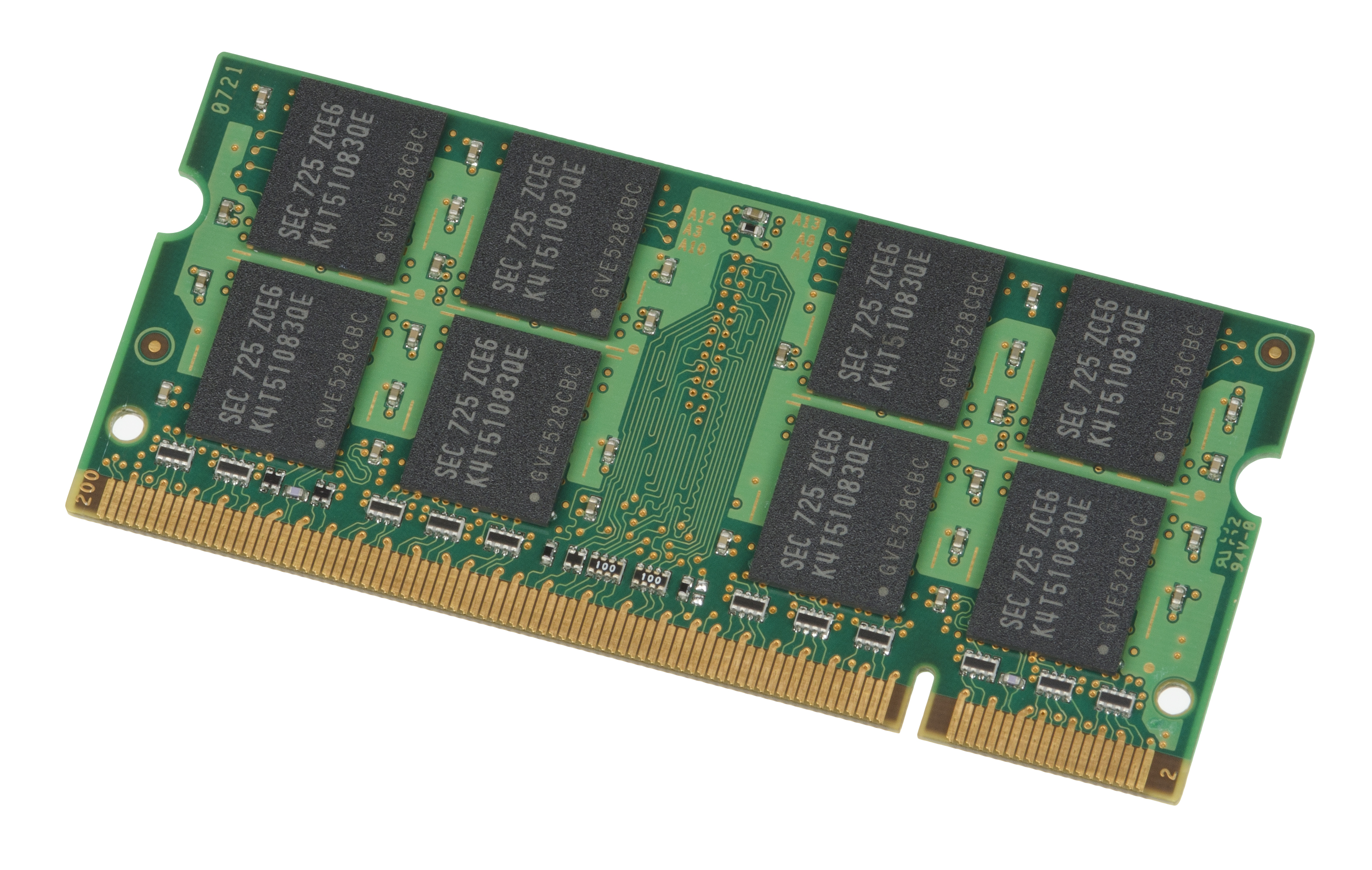
Double Data Rate 3 Synchronous Dynamic Random-Access Memory (DDR3 SDRAM) is a type of synchronous dynamic random-access memory (SDRAM) with a high bandwidth (" double data rate") interface, and has been in use since 2007. It is the higher-speed successor to DDR and DDR2 and predecessor to DDR4 synchronous dynamic random-access memory (SDRAM) chips. DDR3 SDRAM is neither forward nor backward compatible with any earlier type of random-access memory (RAM) because of different signaling voltages, timings, and other factors. DDR3 is a DRAM interface specification. The actual DRAM arrays that store the data are similar to earlier types, with similar performance. The primary benefit of DDR3 SDRAM over its immediate predecessor DDR2 SDRAM, is its ability to transfer data at twice the rate (eight times the speed of its internal memory arrays), enabling higher bandwidth or peak data rates. The DDR3 standard permits DRAM chip capacities of up to 8 gigabits (Gbit), and up to four ranks ... [...More Info...] [...Related Items...] OR: [Wikipedia] [Google] [Baidu] |


.png)

.jpg)


