|
Photo–Dember Effect
In semiconductor physics, the photo–Dember effect (named after its discoverer Harry Dember) is the formation of a charge dipole in the vicinity of a semiconductor surface after ultra-fast photo-generation of charge carriers. The dipole forms owing to the difference of mobilities (or diffusion constants) for holes and electrons which combined with the break of symmetry provided by the surface lead to an effective charge separation in the direction perpendicular to the surface. In an isolated sample, where the macroscopic flow of an electric current is prohibited, the fast carriers (often the electrons) are slowed and the slow carriers (often the holes) are accelerated by an electric field, called the Dember field. One of the main applications of the photo–Dember effect is the generation of terahertz (THz) radiation pulses for terahertz time-domain spectroscopy. This effect is present in most semiconductors but it is particularly strong in narrow-gap semiconductor ... [...More Info...] [...Related Items...] OR: [Wikipedia] [Google] [Baidu] |
Indium Arsenide
Indium arsenide, InAs, or indium monoarsenide, is a narrow-bandgap semiconductor composed of indium and arsenic. It has the appearance of grey cubic crystals with a melting point of 942 °C. Indium arsenide is similar in properties to gallium arsenide and is a direct bandgap material, with a bandgap of 0.35 eV at room temperature. Indium arsenide is used for construction of infrared detectors, for the wavelength range of 1–3.8 µm. The detectors are usually photovoltaic photodiodes. Cryogenically cooled detectors have lower noise, but InAs detectors can be used in higher-power applications at room temperature as well. Indium arsenide is also used for making of diode lasers. InAs is well known for its high electron mobility and narrow energy bandgap. It is widely used as terahertz radiation source as it is a strong photo-Dember emitter. The optoelectronic properties and phonon vibrations are slightly changed under the effect of temperature over the range form 0 K t ... [...More Info...] [...Related Items...] OR: [Wikipedia] [Google] [Baidu] |
Semiconductors
A semiconductor is a material which has an electrical conductivity value falling between that of a conductor, such as copper, and an insulator, such as glass. Its resistivity falls as its temperature rises; metals behave in the opposite way. Its conducting properties may be altered in useful ways by introducing impurities (" doping") into the crystal structure. When two differently doped regions exist in the same crystal, a semiconductor junction is created. The behavior of charge carriers, which include electrons, ions, and electron holes, at these junctions is the basis of diodes, transistors, and most modern electronics. Some examples of semiconductors are silicon, germanium, gallium arsenide, and elements near the so-called "metalloid staircase" on the periodic table. After silicon, gallium arsenide is the second-most common semiconductor and is used in laser diodes, solar cells, microwave-frequency integrated circuits, and others. Silicon is a critical element for fabricat ... [...More Info...] [...Related Items...] OR: [Wikipedia] [Google] [Baidu] |
Photoelectrochemical Process
Photoelectrochemical processes are processes in photoelectrochemistry; they usually involve transforming light into other forms of energy. These processes apply to photochemistry, optically pumped lasers, sensitized solar cells, luminescence, and photochromism. Electron excitation Electron excitation is the movement of an electron to a higher energy state. This can either be done by photoexcitation (PE), where the original electron absorbs the photon and gains all the photon's energy or by electrical excitation (EE), where the original electron absorbs the energy of another, energetic electron. Within a semiconductor crystal lattice, thermal excitation is a process where lattice vibrations provide enough energy to move electrons to a higher energy band. When an excited electron falls back to a lower energy state again, it is called electron relaxation. This can be done by radiation of a photon or giving the energy to a third spectator particle as well. In physics there is a sp ... [...More Info...] [...Related Items...] OR: [Wikipedia] [Google] [Baidu] |
Charge Carriers
In physics, a charge carrier is a particle or quasiparticle that is free to move, carrying an electric charge, especially the particles that carry electric charges in electrical conductors. Examples are electrons, ions and holes. The term is used most commonly in solid state physics. In a conducting medium, an electric field can exert force on these free particles, causing a net motion of the particles through the medium; this is what constitutes an electric current. In conducting media, particles serve to carry charge: *In many metals, the charge carriers are electrons. One or two of the valence electrons from each atom are able to move about freely within the crystal structure of the metal. The free electrons are referred to as conduction electrons, and the cloud of free electrons is called a Fermi gas. Many metals have electron and hole bands. In some, the majority carriers are holes. *In electrolytes, such as salt water, the charge carriers are ions, which are atoms or mo ... [...More Info...] [...Related Items...] OR: [Wikipedia] [Google] [Baidu] |
Acceleration
In mechanics, acceleration is the rate of change of the velocity of an object with respect to time. Accelerations are vector quantities (in that they have magnitude and direction). The orientation of an object's acceleration is given by the orientation of the ''net'' force acting on that object. The magnitude of an object's acceleration, as described by Newton's Second Law, is the combined effect of two causes: * the net balance of all external forces acting onto that object — magnitude is directly proportional to this net resulting force; * that object's mass, depending on the materials out of which it is made — magnitude is inversely proportional to the object's mass. The SI unit for acceleration is metre per second squared (, \mathrm). For example, when a vehicle starts from a standstill (zero velocity, in an inertial frame of reference) and travels in a straight line at increasing speeds, it is accelerating in the direction of travel. If the vehicle turns ... [...More Info...] [...Related Items...] OR: [Wikipedia] [Google] [Baidu] |
Depletion Region
In semiconductor physics, the depletion region, also called depletion layer, depletion zone, junction region, space charge region or space charge layer, is an insulating region within a conductive, doped semiconductor material where the mobile charge carriers have been diffused away, or have been forced away by an electric field. The only elements left in the depletion region are ionized donor or acceptor impurities. This region of uncovered positive and negative ions is called the depletion region due to the depletion of carriers in this region. The depletion region is so named because it is formed from a conducting region by removal of all free charge carriers, leaving none to carry a current. Understanding the depletion region is key to explaining modern semiconductor electronics: diodes, bipolar junction transistors, field-effect transistors, and variable capacitance diodes all rely on depletion region phenomena. Formation in a p–n junction A depletion region ... [...More Info...] [...Related Items...] OR: [Wikipedia] [Google] [Baidu] |
Band Bending
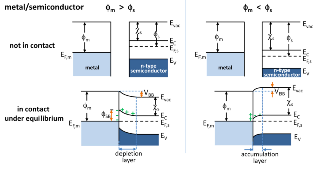
In solid-state physics, band bending refers to the process in which the electronic band structure in a material curves up or down near a junction or interface. It does not involve any physical (spatial) bending. When the electrochemical potential of the free charge carriers around an interface of a semiconductor is dissimilar, charge carriers are transferred between the two materials until an equilibrium state is reached whereby the potential difference vanishes. The band bending concept was first developed in 1938 when Mott, Davidov and Schottky all published theories of the rectifying effect of metal-semiconductor contacts. The use of semiconductor junctions sparked the computer revolution in 1990. Devices such as the diode, the transistor, the photocell and many more still play an important role in technology. Qualitative description Band bending can be induced by several types of contact. In this section metal-semiconductor contact, surface state, applied bias and adsorpti ... [...More Info...] [...Related Items...] OR: [Wikipedia] [Google] [Baidu] |
Fermi Level Pinning
Enrico Fermi (; 29 September 1901 – 28 November 1954) was an Italian (later naturalized American) physicist and the creator of the world's first nuclear reactor, the Chicago Pile-1. He has been called the "architect of the nuclear age" and the "architect of the atomic bomb". He was one of very few physicists to excel in both theoretical physics and experimental physics. Fermi was awarded the 1938 Nobel Prize in Physics for his work on induced radioactivity by neutron bombardment and for the discovery of transuranium elements. With his colleagues, Fermi filed several patents related to the use of nuclear power, all of which were taken over by the US government. He made significant contributions to the development of statistical mechanics, quantum theory, and nuclear and particle physics. Fermi's first major contribution involved the field of statistical mechanics. After Wolfgang Pauli formulated his exclusion principle in 1925, Fermi followed with a paper in which he applie ... [...More Info...] [...Related Items...] OR: [Wikipedia] [Google] [Baidu] |
Electrical Conduction
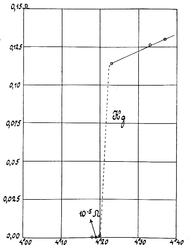
Electrical resistivity (also called specific electrical resistance or volume resistivity) is a fundamental property of a material that measures how strongly it resists electric current. A low resistivity indicates a material that readily allows electric current. Resistivity is commonly represented by the Greek letter (rho). The SI unit of electrical resistivity is the ohm-meter (Ω⋅m). For example, if a solid cube of material has sheet contacts on two opposite faces, and the resistance between these contacts is , then the resistivity of the material is . Electrical conductivity or specific conductance is the reciprocal of electrical resistivity. It represents a material's ability to conduct electric current. It is commonly signified by the Greek letter (sigma), but (kappa) (especially in electrical engineering) and ( gamma) are sometimes used. The SI unit of electrical conductivity is siemens per metre (S/m). Resistivity and conductivity are inte ... [...More Info...] [...Related Items...] OR: [Wikipedia] [Google] [Baidu] |
Valence (chemistry)
In chemistry, the valence (US spelling) or valency (British spelling) of an element is the measure of its combining capacity with other atoms when it forms chemical compounds or molecules. Description The combining capacity, or affinity of an atom of a given element is determined by the number of hydrogen atoms that it combines with. In methane, carbon has a valence of 4; in ammonia, nitrogen has a valence of 3; in water, oxygen has a valence of 2; and in hydrogen chloride, chlorine has a valence of 1. Chlorine, as it has a valence of one, can be substituted for hydrogen. Phosphorus has a valence of 5 in phosphorus pentachloride, . Valence diagrams of a compound represent the connectivity of the elements, with lines drawn between two elements, sometimes called bonds, representing a saturated valency for each element. The two tables below show some examples of different compounds, their valence diagrams, and the valences for each element of the compound. Modern definitions ... [...More Info...] [...Related Items...] OR: [Wikipedia] [Google] [Baidu] |
Energy Band
In solid-state physics, the electronic band structure (or simply band structure) of a solid describes the range of energy levels that electrons may have within it, as well as the ranges of energy that they may not have (called ''band gaps'' or ''forbidden bands''). Band theory derives these bands and band gaps by examining the allowed quantum mechanical wave functions for an electron in a large, periodic lattice of atoms or molecules. Band theory has been successfully used to explain many physical properties of solids, such as electrical resistivity and optical absorption, and forms the foundation of the understanding of all solid-state devices (transistors, solar cells, etc.). Why bands and band gaps occur The electrons of a single, isolated atom occupy atomic orbitals each of which has a discrete energy level. When two or more atoms join together to form a molecule, their atomic orbitals overlap and hybridize. Similarly, if a large number ''N'' of identical atoms come ... [...More Info...] [...Related Items...] OR: [Wikipedia] [Google] [Baidu] |


