|
Lead Frame
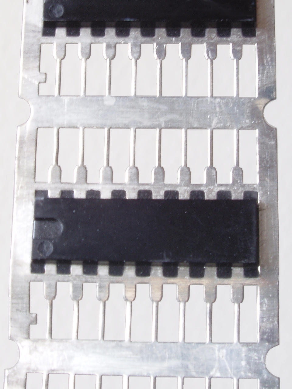
A lead frame (pronounced ) is the metal structure inside a chip package that carries signals from the die to the outside. The lead frame consists of a central die pad, where the die is placed, surrounded by leads, metal conductors leading away from the die to the outside world. The end of each lead closest to the die ends in a bond pad. Small bond wires connect the die to each bond pad. Mechanical connections fix all these parts into a rigid structure, which makes the whole lead frame easy to handle automatically. Manufacturing Lead frames are manufactured by removing material from a flat plate of copper, copper-alloy, or iron-nickel alloy like alloy 42. Two processes used for this are etching (suitable for high density of leads), or stamping (suitable for low density of leads). The mechanical bending process can be applied after both techniques. The die is glued or soldered to the die pad inside the lead frame, and then bond wires are attached between the die and the bond p ... [...More Info...] [...Related Items...] OR: [Wikipedia] [Google] [Baidu] |
TQFP Leadframe
A quad flat package (QFP) is a surface-mounted integrated circuit package with "gull wing" leads extending from each of the four sides. Socketing such packages is rare and through-hole mounting is not possible. Versions ranging from 32 to 304 pins with a pitch ranging from 0.4 to 1.0 mm are common. Other special variants include low-profile QFP (LQFP) and thin QFP (TQFP). The QFP component package type became common in Europe and United States during the early nineties, even though it has been used in Japanese consumer electronics since the seventies. It is often mixed with hole mounted, and sometimes socketed, components on the same printed circuit board (PCB). A package related to QFP is plastic leaded chip carrier (PLCC) which is similar but has pins with larger pitch, 1.27 mm (or 1/20 inch), curved up underneath a thicker body to simplify socketing (soldering is also possible). It is commonly used for NOR flash memories and other programmable component ... [...More Info...] [...Related Items...] OR: [Wikipedia] [Google] [Baidu] |
Wire Bonding
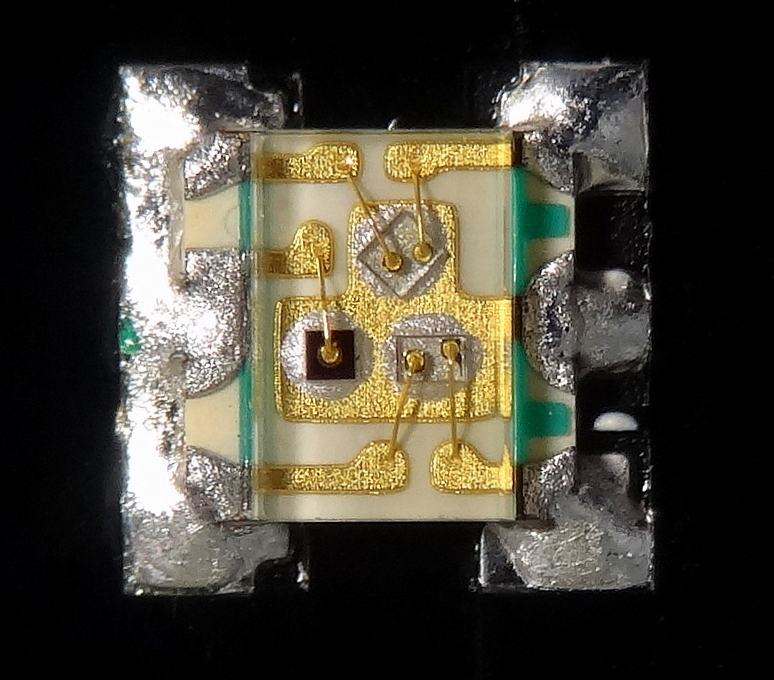
Wire bonding is the method of making interconnections between an integrated circuit (IC) or other semiconductor device and its packaging during semiconductor device fabrication. Although less common, wire bonding can be used to connect an IC to other electronics or to connect from one printed circuit board (PCB) to another. Wire bonding is generally considered the most cost-effective and flexible interconnect technology and is used to assemble the vast majority of semiconductor packages. Wire bonding can be used at frequencies above 100 GHz. [...More Info...] [...Related Items...] OR: [Wikipedia] [Google] [Baidu] |
Quad Flat No-leads Package
Flat no-leads packages such as quad-flat no-leads (QFN) and dual-flat no-leads (DFN) physically and electrically connect integrated circuits to printed circuit boards. Flat no-leads, also known as micro leadframe (MLF) and SON (small-outline no leads), is a surface-mount technology, one of several package technologies that connect ICs to the ''surfaces'' of PCBs without through-holes. Flat no-lead is a near chip scale plastic encapsulated package made with a planar copper lead frame substrate. Perimeter lands on the package bottom provide electrical connections to the PCB. Flat no-lead packages include an exposed thermally conductive pad to improve heat transfer out of the IC (into the PCB). Heat transfer can be further facilitated by metal vias in the thermal pad. The QFN package is similar to the quad-flat package (QFP), and a ball grid array (BGA). Flat no-lead cross-section The figure shows the cross section of a flat no-lead package with a lead frame and wire bon ... [...More Info...] [...Related Items...] OR: [Wikipedia] [Google] [Baidu] |
Quad Flat Package
A quad flat package (QFP) is a surface-mounted integrated circuit package with "gull wing" leads extending from each of the four sides. Socketing such packages is rare and through-hole mounting is not possible. Versions ranging from 32 to 304 pins with a pitch ranging from 0.4 to 1.0 mm are common. Other special variants include low-profile QFP (LQFP) and thin QFP (TQFP). The QFP component package type became common in Europe and United States during the early nineties, even though it has been used in Japanese consumer electronics since the seventies. It is often mixed with hole mounted, and sometimes socketed, components on the same printed circuit board (PCB). A package related to QFP is plastic leaded chip carrier (PLCC) which is similar but has pins with larger pitch, 1.27 mm (or 1/20 inch), curved up underneath a thicker body to simplify socketing (soldering is also possible). It is commonly used for NOR flash memories and other programmable components. ... [...More Info...] [...Related Items...] OR: [Wikipedia] [Google] [Baidu] |
Dual In-line Package
In microelectronics, a dual in-line package (DIP or DIL), is an electronic component package with a rectangular housing and two parallel rows of electrical connecting pins. The package may be through-hole mounted to a printed circuit board (PCB) or inserted in a socket. The dual-inline format was invented by Don Forbes, Rex Rice and Bryant Rogers at Fairchild R&D in 1964, when the restricted number of leads available on circular transistor-style packages became a limitation in the use of integrated circuits. Increasingly complex circuits required more signal and power supply leads (as observed in Rent's rule); eventually microprocessors and similar complex devices required more leads than could be put on a DIP package, leading to development of higher-density chip carriers. Furthermore, square and rectangular packages made it easier to route printed-circuit traces beneath the packages. A DIP is usually referred to as a DIP''n'', where ''n'' is the total number of pins. For ... [...More Info...] [...Related Items...] OR: [Wikipedia] [Google] [Baidu] |
Chip Carrier
In electronics, a chip carrier is one of several kinds of surface-mount technology packages for integrated circuits (commonly called "chips"). Connections are made on all four edges of a square package; compared to the internal cavity for mounting the integrated circuit, the package overall size is large.Kenneth Jackson, Wolfgang Schroter, (ed), ''Handbook of Semiconductor Technology Volume 2'',Wiley VCH, 2000, ,page 627 Types Chip carriers may have either J-shaped metal leads for connections by solder or by a socket, or may be lead-less with metal pads for connections. If the leads extend beyond the package, the preferred description is " flat pack". Chip carriers can be smaller than dual in-line packages and since they use all four edges of the package they can have a larger pin count. Chip carriers may be made of ceramic or plastic. Some forms of chip carrier package are standardized in dimensions and registered with trade industry associations such as JEDEC. Other forms ar ... [...More Info...] [...Related Items...] OR: [Wikipedia] [Google] [Baidu] |


