|
HEMT
A high-electron-mobility transistor (HEMT), also known as heterostructure FET (HFET) or modulation-doped FET (MODFET), is a field-effect transistor incorporating a junction between two materials with different band gaps (i.e. a heterojunction) as the channel instead of a doped region (as is generally the case for a MOSFET). A commonly used material combination is GaAs with AlGaAs, though there is wide variation, dependent on the application of the device. Devices incorporating more indium generally show better high-frequency performance, while in recent years, gallium nitride HEMTs have attracted attention due to their high-power performance. Like other FETs, HEMTs are used in integrated circuits as digital on-off switches. FETs can also be used as amplifiers for large amounts of current using a small voltage as a control signal. Both of these uses are made possible by the FET’s unique current–voltage characteristics. HEMT transistors are able to operate at higher frequenci ... [...More Info...] [...Related Items...] OR: [Wikipedia] [Google] [Baidu] |
Gallium Nitride
Gallium nitride () is a binary III/ V direct bandgap semiconductor commonly used in blue light-emitting diodes since the 1990s. The compound is a very hard material that has a Wurtzite crystal structure. Its wide band gap of 3.4 eV affords it special properties for applications in optoelectronic, high-power and high-frequency devices. For example, GaN is the substrate which makes violet (405 nm) laser diodes possible, without requiring nonlinear optical frequency-doubling. Its sensitivity to ionizing radiation is low (like other group III nitrides), making it a suitable material for solar cell arrays for satellites. Military and space applications could also benefit as devices have shown stability in high radiation environments. Because GaN transistors can operate at much higher temperatures and work at much higher voltages than gallium arsenide (GaAs) transistors, they make ideal power amplifiers at microwave frequencies. In addition, GaN offers promising characteris ... [...More Info...] [...Related Items...] OR: [Wikipedia] [Google] [Baidu] |
Heterojunction
A heterojunction is an interface between two layers or regions of dissimilar semiconductors. These semiconducting materials have unequal band gaps as opposed to a homojunction. It is often advantageous to engineer the electronic energy bands in many solid-state device applications, including semiconductor lasers, solar cells and transistors. The combination of multiple heterojunctions together in a device is called a heterostructure, although the two terms are commonly used interchangeably. The requirement that each material be a semiconductor with unequal band gaps is somewhat loose, especially on small length scales, where electronic properties depend on spatial properties. A more modern definition of heterojunction is the interface between any two solid-state materials, including crystalline and amorphous structures of metallic, insulating, fast ion conductor and semiconducting materials. Manufacture and applications Heterojunction manufacturing generally requires the use of mo ... [...More Info...] [...Related Items...] OR: [Wikipedia] [Google] [Baidu] |
Gallium Arsenide
Gallium arsenide (GaAs) is a III-V direct band gap semiconductor with a Zincblende (crystal structure), zinc blende crystal structure. Gallium arsenide is used in the manufacture of devices such as microwave frequency integrated circuits, monolithic microwave integrated circuits, infrared light-emitting diodes, laser diodes, solar cells and optical windows. GaAs is often used as a substrate material for the epitaxial growth of other III-V semiconductors, including indium gallium arsenide, aluminum gallium arsenide and others. Preparation and chemistry In the compound, gallium has a +3 oxidation state. Gallium arsenide single crystals can be prepared by three industrial processes: * The vertical gradient freeze (VGF) process. * Crystal growth using a horizontal zone furnace in the Bridgman-Stockbarger technique, in which gallium and arsenic vapors react, and free molecules deposit on a seed crystal at the cooler end of the furnace. * Liquid encapsulated Czochralski process, Czoch ... [...More Info...] [...Related Items...] OR: [Wikipedia] [Google] [Baidu] |
GaAs
Gallium arsenide (GaAs) is a III-V direct band gap semiconductor with a zinc blende crystal structure. Gallium arsenide is used in the manufacture of devices such as microwave frequency integrated circuits, monolithic microwave integrated circuits, infrared light-emitting diodes, laser diodes, solar cells and optical windows. GaAs is often used as a substrate material for the epitaxial growth of other III-V semiconductors, including indium gallium arsenide, aluminum gallium arsenide and others. Preparation and chemistry In the compound, gallium has a +3 oxidation state. Gallium arsenide single crystals can be prepared by three industrial processes: * The vertical gradient freeze (VGF) process. * Crystal growth using a horizontal zone furnace in the Bridgman-Stockbarger technique, in which gallium and arsenic vapors react, and free molecules deposit on a seed crystal at the cooler end of the furnace. * Liquid encapsulated Czochralski (LEC) growth is used for producing high-puri ... [...More Info...] [...Related Items...] OR: [Wikipedia] [Google] [Baidu] |
Field-effect Transistor
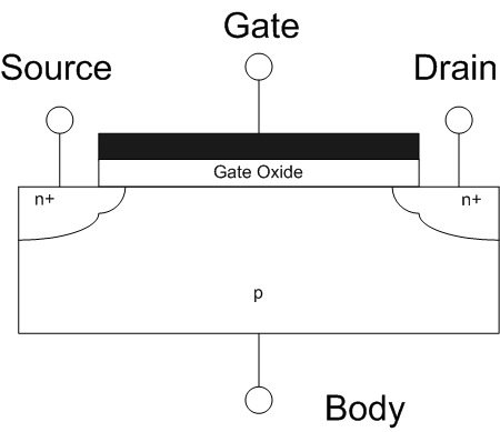
The field-effect transistor (FET) is a type of transistor that uses an electric field to control the flow of current in a semiconductor. FETs (JFETs or MOSFETs) are devices with three terminals: ''source'', ''gate'', and ''drain''. FETs control the flow of current by the application of a voltage to the gate, which in turn alters the conductivity between the drain and source. FETs are also known as unipolar transistors since they involve single-carrier-type operation. That is, FETs use either electrons (n-channel) or holes (p-channel) as charge carriers in their operation, but not both. Many different types of field effect transistors exist. Field effect transistors generally display very high input impedance at low frequencies. The most widely used field-effect transistor is the MOSFET (metal-oxide-semiconductor field-effect transistor). History The concept of a field-effect transistor (FET) was first patented by Austro-Hungarian physicist Julius Edgar Lilienfeld in 192 ... [...More Info...] [...Related Items...] OR: [Wikipedia] [Google] [Baidu] |
Patent
A patent is a type of intellectual property that gives its owner the legal right to exclude others from making, using, or selling an invention for a limited period of time in exchange for publishing an enabling disclosure of the invention."A patent is not the grant of a right to make or use or sell. It does not, directly or indirectly, imply any such right. It grants only the right to exclude others. The supposition that a right to make is created by the patent grant is obviously inconsistent with the established distinctions between generic and specific patents, and with the well-known fact that a very considerable portion of the patents granted are in a field covered by a former relatively generic or basic patent, are tributary to such earlier patent, and cannot be practiced unless by license thereunder." – ''Herman v. Youngstown Car Mfg. Co.'', 191 F. 579, 584–85, 112 CCA 185 (6th Cir. 1911) In most countries, patent rights fall under private law and the patent holder mus ... [...More Info...] [...Related Items...] OR: [Wikipedia] [Google] [Baidu] |
Superlattice
A superlattice is a periodic structure of layers of two (or more) materials. Typically, the thickness of one layer is several nanometers. It can also refer to a lower-dimensional structure such as an array of quantum dots or quantum wells. Discovery Superlattices were discovered early in 1925 by Johansson and Linde after the studies on gold-copper and palladium-copper systems through their special X-ray diffraction patterns. Further experimental observations and theoretical modifications on the field were done by Bradley and Jay, Gorsky, Borelius, Dehlinger and Graf, Bragg and Williams and Bethe. Theories were based on the transition of arrangement of atoms in crystal lattices from disordered state to an ordered state. Mechanical properties J.S. Koehler theoretically predicted that by using alternate (nano-)layers of materials with high and low elastic constants, shearing resistance is improved by up to 100 times as the Frank–Read source of dislocations cannot operate in ... [...More Info...] [...Related Items...] OR: [Wikipedia] [Google] [Baidu] |
Bell Labs
Nokia Bell Labs, originally named Bell Telephone Laboratories (1925–1984), then AT&T Bell Laboratories (1984–1996) and Bell Labs Innovations (1996–2007), is an American industrial research and scientific development company owned by multinational company Nokia. With headquarters located in Murray Hill, New Jersey, the company operates several laboratories in the United States and around the world. Researchers working at Bell Laboratories are credited with the development of radio astronomy, the transistor, the laser, the photovoltaic cell, the charge-coupled device (CCD), information theory, the Unix operating system, and the programming languages B, C, C++, S, SNOBOL, AWK, AMPL, and others. Nine Nobel Prizes have been awarded for work completed at Bell Laboratories. Bell Labs had its origin in the complex corporate organization of the Bell System telephone conglomerate. In the late 19th century, the laboratory began as the Western Electric Engineering Department, l ... [...More Info...] [...Related Items...] OR: [Wikipedia] [Google] [Baidu] |
Arthur Gossard
Arthur C. Gossard was a professor of materials and electrical engineering at the University of California, Santa Barbara. In 1982, he co-discovered the fractional quantum Hall effect. His research is related to molecular beam epitaxy (MBE). He has a doctorate in physics from UC Berkeley. After university, he joined Bell Labs. In 1987, he was elected a member of the US National Academy of Engineering for contributions to the study of the physics of ultra-thin semiconducting layers through molecular beam epitaxy, leading to new physics and new devices. He was also a member of the US National Academy of Sciences. In 2016, Gossard was named as a recipient of a National Medal of Technology and Innovation The National Medal of Technology and Innovation (formerly the National Medal of Technology) is an honor granted by the President of the United States to American inventors and innovators who have made significant contributions to the development .... He died on 26 June 2022. Refer ... [...More Info...] [...Related Items...] OR: [Wikipedia] [Google] [Baidu] |
Horst Störmer
Horst may refer to: Science * Horst (geology), a raised fault block bounded by normal faults or graben People * Horst (given name) * Horst (surname) * ter Horst, Dutch surname * van der Horst, Dutch surname Places Settlements Germany * Horst, Steinburg, a municipality in the district of Steinburg in Schleswig-Holstein * Horst, Lauenburg, a municipality in the district of Lauenburg in Schleswig-Holstein * Horst, Mecklenburg-Vorpommern, a village and district in the municipality of Sundhagen, Mecklenburg-Vorpommern * , a district in the city of Gelsenkirchen, North Rhine-Westphalia * , a town in the municipality of Seevetal, Lower Saxony Netherlands * Horst aan de Maas, a municipality in the province of Limburg ** Horst, Limburg, the municipal seat of Horst aan de Maas * , a hamlet in the municipality of Ermelo, Gelderland * , a village in the municipality of Gilze en Rijen, North Brabant * Schothorst, , and , districts in the city and municipality of Amersfoort, Utrecht Polan ... [...More Info...] [...Related Items...] OR: [Wikipedia] [Google] [Baidu] |
Thomson-CSF
Thomson-CSF was a French company that specialized in the development and manufacture of electronics with a heavy focus upon the aerospace and defence sectors of the market. Thomson-CSF was formed in 1968 following the merger of Thomson-Houston-Hotchkiss-Brandt with the Compagnie Générale de Télégraphie Sans Fil (''General Wireless Telegraphy Company'', commonly abbreviated as ''CSF''), these two companies being the source of the name ''Thomson-CSF''. It operated as an electronics specialist on products such as broadcasting equipment, electroacoustics, shortwave radio sets, radar systems and television. During the 1970s, the company diversified manufacturing backend telephony equipment, semiconductors, and medical imaging apparatus. It also entered into large deals outside of the domestic market, acquiring considerable business in the Middle East. During the late 1980s, Thomson-CSF, anticipating defence spending cutbacks, conducted a radical business restructuring, mergi ... [...More Info...] [...Related Items...] OR: [Wikipedia] [Google] [Baidu] |


