|
Germanium-vacancy Center In Diamond
The germanium-vacancy center (Ge-V) is an optically active Crystallographic defects in diamond, defect in diamond, which can be created by doping germanium into diamond during its growth or by implanting germanium ions into diamond after its growth. Its properties are similar to those of the silicon-vacancy center in diamond (SiV). Ge-V can behave as a single-photon source and shows potential for quantum and nanoscience applications due to its narrow Zero-phonon line and phonon sideband, zero-phonon line (ZPL) and minimal phononic-sideband (compared to that of the nitrogen-vacancy center (NV)). Properties Ge-V is predicted to consist of one germanium atom situated between two adjacent lattice vacancies and have the same D3d Crystallographic point group, point group symmetry as SiV. It has a single ZPL at 602 nm (2.059 eV) at room-temperature, which splits into two components separated by 0.67 meV at low-temperatures (10 K). The Ge-V has an excited state li ... [...More Info...] [...Related Items...] OR: [Wikipedia] [Google] [Baidu] |
Nitrogen-vacancy Center
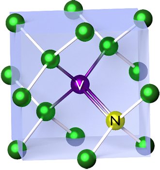
The nitrogen-vacancy center (N-V center or NV center) is one of numerous point defects in diamond. Its most explored and useful property is its photoluminescence, which allows observers to read out its spin-state. The NV center's electron spin, localized at atomic scales, can be manipulated at room temperature by external factors such as magnetic, or electric fields, microwave radiation, or light, resulting in sharp resonances in the intensity of the photoluminescence. These resonances can be explained in terms of electron spin related phenomena such as quantum entanglement, spin–orbit interaction and Rabi oscillations, and analysed using advanced quantum optics theory. An individual NV center can be used as a basic unit for a quantum computer, a qubit, and used for quantum cryptography. Further potential applications in novel fields of electronics and sensing include spintronics, masers, and quantum sensors. If the charge is not specified the term "NV center" refers to the negativ ... [...More Info...] [...Related Items...] OR: [Wikipedia] [Google] [Baidu] |
Spectroscopy
Spectroscopy is the field of study that measures and interprets the electromagnetic spectra that result from the interaction between electromagnetic radiation and matter as a function of the wavelength or frequency of the radiation. Matter waves and acoustic waves can also be considered forms of radiative energy, and recently gravitational waves have been associated with a spectral signature in the context of the Laser Interferometer Gravitational-Wave Observatory (LIGO) In simpler terms, spectroscopy is the precise study of color as generalized from visible light to all bands of the electromagnetic spectrum. Historically, spectroscopy originated as the study of the wavelength dependence of the absorption by gas phase matter of visible light dispersed by a prism. Spectroscopy, primarily in the electromagnetic spectrum, is a fundamental exploratory tool in the fields of astronomy, chemistry, materials science, and physics, allowing the composition, physical structure and e ... [...More Info...] [...Related Items...] OR: [Wikipedia] [Google] [Baidu] |
Spintronics
Spintronics (a portmanteau meaning spin transport electronics), also known as spin electronics, is the study of the intrinsic spin of the electron and its associated magnetic moment, in addition to its fundamental electronic charge, in solid-state devices. The field of spintronics concerns spin-charge coupling in metallic systems; the analogous effects in insulators fall into the field of multiferroics. Spintronics fundamentally differs from traditional electronics in that, in addition to charge state, electron spins are exploited as a further degree of freedom, with implications in the efficiency of data storage and transfer. Spintronic systems are most often realised in dilute magnetic semiconductors (DMS) and Heusler alloys and are of particular interest in the field of quantum computing and neuromorphic computing. History Spintronics emerged from discoveries in the 1980s concerning spin-dependent electron transport phenomena in solid-state devices. This includes the observa ... [...More Info...] [...Related Items...] OR: [Wikipedia] [Google] [Baidu] |
Diamond
Diamond is a Allotropes of carbon, solid form of the element carbon with its atoms arranged in a crystal structure called diamond cubic. Another solid form of carbon known as graphite is the Chemical stability, chemically stable form of carbon at Standard conditions for temperature and pressure, room temperature and pressure, but diamond is metastable and converts to it at a negligible rate under those conditions. Diamond has the highest Scratch hardness, hardness and thermal conductivity of any natural material, properties that are used in major industrial applications such as cutting and polishing tools. They are also the reason that diamond anvil cells can subject materials to pressures found deep in the Earth. Because the arrangement of atoms in diamond is extremely rigid, few types of impurity can contaminate it (two exceptions are boron and nitrogen). Small numbers of lattice defect, defects or impurities (about one per million of lattice atoms) color diamond blue (bor ... [...More Info...] [...Related Items...] OR: [Wikipedia] [Google] [Baidu] |
Annealing (metallurgy)
In metallurgy and materials science, annealing is a heat treatment that alters the physical and sometimes chemical properties of a material to increase its ductility and reduce its hardness, making it more workable. It involves heating a material above its recrystallization temperature, maintaining a suitable temperature for an appropriate amount of time and then cooling. In annealing, atoms migrate in the crystal lattice and the number of dislocations decreases, leading to a change in ductility and hardness. As the material cools it recrystallizes. For many alloys, including carbon steel, the crystal grain size and phase composition, which ultimately determine the material properties, are dependent on the heating rate and cooling rate. Hot working or cold working after the annealing process alters the metal structure, so further heat treatments may be used to achieve the properties required. With knowledge of the composition and phase diagram, heat treatment can be used to ad ... [...More Info...] [...Related Items...] OR: [Wikipedia] [Google] [Baidu] |
Ion Implantation
Ion implantation is a low-temperature process by which ions of one element are accelerated into a solid target, thereby changing the physical, chemical, or electrical properties of the target. Ion implantation is used in semiconductor device fabrication and in metal finishing, as well as in materials science research. The ions can alter the elemental composition of the target (if the ions differ in composition from the target) if they stop and remain in the target. Ion implantation also causes chemical and physical changes when the ions impinge on the target at high energy. The crystal structure of the target can be damaged or even destroyed by the energetic collision cascades, and ions of sufficiently high energy (10s of MeV) can cause nuclear transmutation. General principle Ion implantation equipment typically consists of an ion source, where ions of the desired element are produced, an accelerator, where the ions are electrostatically accelerated to a high energy, and ... [...More Info...] [...Related Items...] OR: [Wikipedia] [Google] [Baidu] |
Crystallographic Point Group
In crystallography, a crystallographic point group is a set of symmetry operations, corresponding to one of the point groups in three dimensions, such that each operation (perhaps followed by a translation) would leave the structure of a crystal unchanged i.e. the same kinds of atoms would be placed in similar positions as before the transformation. For example, in many crystals in the cubic crystal system, a rotation of the unit cell by 90 degrees around an axis that is perpendicular to one of the faces of the cube is a symmetry operation that moves each atom to the location of another atom of the same kind, leaving the overall structure of the crystal unaffected. In the classification of crystals, each point group defines a so-called (geometric) crystal class. There are infinitely many three-dimensional point groups. However, the crystallographic restriction on the general point groups results in there being only 32 crystallographic point groups. These 32 point groups are one-and ... [...More Info...] [...Related Items...] OR: [Wikipedia] [Google] [Baidu] |
Zero-phonon Line And Phonon Sideband
The zero-phonon line and the phonon sideband jointly constitute the line shape of individual light absorbing and emitting molecules ( chromophores) embedded into a transparent solid matrix. When the host matrix contains many chromophores, each will contribute a zero- phonon line and a phonon sideband to the absorption and emission spectra. The spectra originating from a collection of identical chromophores in a matrix is said to be inhomogeneously broadened because each chromophore is surrounded by a somewhat different matrix environment which modifies the energy required for an electronic transition. In an inhomogeneous distribution of chromophores, individual zero-phonon line and phonon sideband positions are therefore shifted and overlapping. Figure 1 shows the typical line shape for electronic transitions of individual chromophores in a solid matrix. The zero-phonon line is located at a frequency ω’ determined by the intrinsic difference in energy levels between ground an ... [...More Info...] [...Related Items...] OR: [Wikipedia] [Google] [Baidu] |
Single-photon Source
Single-photon sources are light sources that emit light as single particles or photons. These sources are distinct from coherent light sources (lasers) and thermal light sources such as incandescent light bulbs. The Heisenberg uncertainty principle dictates that a state with an exact number of photons of a single frequency cannot be created. However, Fock states (or number states) can be studied for a system where the electric field amplitude is distributed over a narrow bandwidth. In this context, a single-photon source gives rise to an effectively one-photon number state. Photons from an ideal single-photon source exhibit quantum mechanical characteristics. These characteristics include photon antibunching, so that the time between two successive photons is never less than some minimum value. This behaviour is normally demonstrated by using a beam splitter to direct about half of the incident photons toward one avalanche photodiode, and half toward a second. Pulses from one detecto ... [...More Info...] [...Related Items...] OR: [Wikipedia] [Google] [Baidu] |
Silicon-vacancy Center In Diamond
The silicon-vacancy center (Si-V) is an optically active defect in diamond (referred to as a color center) that is receiving an increasing amount of interest in the diamond research community. This interest is driven primarily by the coherent optical properties of the Si-V, especially compared to the well-known and extensively-studied nitrogen-vacancy center (N-V). Properties Crystallographic The Si-V center is formed by replacing two neighboring carbon atoms in the diamond lattice with one silicon atom, which places itself between the two vacant lattice sites. This configuration has a D3d point group symmetry. Electronic The Si-V center is a single-hole (spin-1/2) system with ground and excited electronic states located within the diamond bandgap. The ground and excited electronic states have two orbital states split by spin–orbit coupling. Each of these spin–orbit states is doubly degenerate by spin, and this splitting can be affected by lattice strain. Phonons ... [...More Info...] [...Related Items...] OR: [Wikipedia] [Google] [Baidu] |


.png)