|
Dry Etching
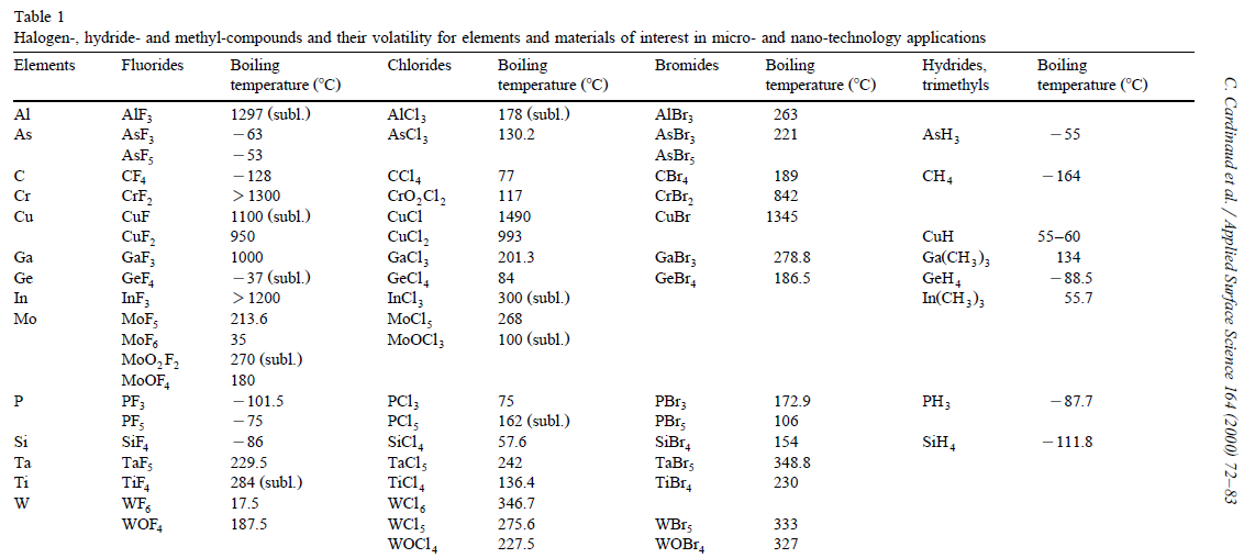
Dry etching refers to the removal of material, typically a masked pattern of semiconductor material, by exposing the material to a bombardment of ions (usually a plasma of reactive gases such as fluorocarbons, oxygen, chlorine, boron trichloride; sometimes with addition of nitrogen, argon, helium and other gases) that dislodge portions of the material from the exposed surface. A common type of dry etching is reactive-ion etching. Unlike with many (but not all, see isotropic etching) of the wet chemical etchants used in wet etching, the dry etching process typically etches directionally or anisotropically. Applications Dry etching is used in conjunction with photolithographic techniques to attack certain areas of a semiconductor surface in order to form recesses in material. Applications include contact holes (which are contacts to the underlying semiconductor substrate), via holes (which are holes that are formed to provide an interconnect path between conductive layers in th ... [...More Info...] [...Related Items...] OR: [Wikipedia] [Google] [Baidu] |
Semiconductor
A semiconductor is a material which has an electrical resistivity and conductivity, electrical conductivity value falling between that of a electrical conductor, conductor, such as copper, and an insulator (electricity), insulator, such as glass. Its electrical resistivity and conductivity, resistivity falls as its temperature rises; metals behave in the opposite way. Its conducting properties may be altered in useful ways by introducing impurities ("doping (semiconductor), doping") into the crystal structure. When two differently doped regions exist in the same crystal, a semiconductor junction is created. The behavior of charge carriers, which include electrons, ions, and electron holes, at these junctions is the basis of diodes, transistors, and most modern electronics. Some examples of semiconductors are silicon, germanium, gallium arsenide, and elements near the so-called "metalloid staircase" on the periodic table. After silicon, gallium arsenide is the second-most common s ... [...More Info...] [...Related Items...] OR: [Wikipedia] [Google] [Baidu] |
Microelectromechanical Systems
Microelectromechanical systems (MEMS), also written as micro-electro-mechanical systems (or microelectronic and microelectromechanical systems) and the related micromechatronics and microsystems constitute the technology of microscopic devices, particularly those with moving parts. They merge at the nanoscale into nanoelectromechanical systems (NEMS) and nanotechnology. MEMS are also referred to as micromachines in Japan and microsystem technology (MST) in Europe. MEMS are made up of components between 1 and 100 micrometers in size (i.e., 0.001 to 0.1 mm), and MEMS devices generally range in size from 20 micrometres to a millimetre (i.e., 0.02 to 1.0 mm), although components arranged in arrays (e.g., digital micromirror devices) can be more than 1000 mm2. They usually consist of a central unit that processes data (an integrated circuit chip such as microprocessor) and several components that interact with the surroundings (such as microsensors). Because of the la ... [...More Info...] [...Related Items...] OR: [Wikipedia] [Google] [Baidu] |
MOSFET
The metal–oxide–semiconductor field-effect transistor (MOSFET, MOS-FET, or MOS FET) is a type of field-effect transistor (FET), most commonly fabricated by the controlled oxidation of silicon. It has an insulated gate, the voltage of which determines the conductivity of the device. This ability to change conductivity with the amount of applied voltage can be used for amplifying or switching electronic signals. A metal-insulator-semiconductor field-effect transistor (MISFET) is a term almost synonymous with MOSFET. Another synonym is IGFET for insulated-gate field-effect transistor. The basic principle of the field-effect transistor was first patented by Julius Edgar Lilienfeld in 1925.Lilienfeld, Julius Edgar (1926-10-08) "Method and apparatus for controlling electric currents" upright=1.6, Two power MOSFETs in V_in_the_''off''_state,_and_can_conduct_a_continuous_current_of_30 surface-mount_packages._Operating_as_switches,_each_of_these_components_can_su ... [...More Info...] [...Related Items...] OR: [Wikipedia] [Google] [Baidu] |
List Of Semiconductor Scale Examples
Listed are many semiconductor scale examples for various metal–oxide–semiconductor field-effect transistor (MOSFET, or MOS transistor) semiconductor manufacturing process nodes. Timeline of MOSFET demonstrations PMOS and NMOS CMOS (single-gate) Multi-gate MOSFET (MuGFET) Other types of MOSFET Commercial products using micro-scale MOSFETs Products featuring 20 μm manufacturing process * RCA's CD4000 series of integrated circuits (ICs) beginning in 1968. Products featuring 10 μm manufacturing process * Intel 4004, the first single-chip microprocessor CPU, launched in 1971. * Intel 8008 CPU launched in 1972. * MOS Technology 6502 1 MHz CPU launched in 1975 (8 μm). Products featuring 8 μm manufacturing process * Intel 1103, an early dynamic random-access memory (DRAM) chip launched in 1970. Products featuring 6 μm manufacturing process * Toshiba TLCS-12, a microprocessor developed for the Ford EEC (Electronic Engine C ... [...More Info...] [...Related Items...] OR: [Wikipedia] [Google] [Baidu] |
Semiconductor Device Fabrication
Semiconductor device fabrication is the process used to manufacture semiconductor devices, typically integrated circuit (IC) chips such as modern computer processors, microcontrollers, and memory chips such as NAND flash and DRAM that are present in everyday electrical and electronics, electronic devices. It is a multiple-step sequence of Photolithography, photolithographic and chemical processing steps (such as surface passivation, thermal oxidation, planar process, planar diffusion and p–n junction isolation, junction isolation) during which electronic circuits are gradually created on a wafer (electronics), wafer made of pure semiconducting material. Silicon is almost always used, but various compound semiconductors are used for specialized applications. The entire manufacturing process takes time, from start to packaged chips ready for shipment, at least six to eight weeks (tape-out only, not including the circuit design) and is performed in highly specialized semiconduct ... [...More Info...] [...Related Items...] OR: [Wikipedia] [Google] [Baidu] |
Robert H
The name Robert is an ancient Germanic given name, from Proto-Germanic "fame" and "bright" (''Hrōþiberhtaz''). Compare Old Dutch ''Robrecht'' and Old High German ''Hrodebert'' (a compound of '' Hruod'' ( non, Hróðr) "fame, glory, honour, praise, renown" and ''berht'' "bright, light, shining"). It is the second most frequently used given name of ancient Germanic origin. It is also in use as a surname. Another commonly used form of the name is Rupert. After becoming widely used in Continental Europe it entered England in its Old French form ''Robert'', where an Old English cognate form (''Hrēodbēorht'', ''Hrodberht'', ''Hrēodbēorð'', ''Hrœdbœrð'', ''Hrœdberð'', ''Hrōðberχtŕ'') had existed before the Norman Conquest. The feminine version is Roberta. The Italian, Portuguese, and Spanish form is Roberto. Robert is also a common name in many Germanic languages, including English, German, Dutch, Norwegian, Swedish, Scots, Danish, and Icelandic. It can be use ... [...More Info...] [...Related Items...] OR: [Wikipedia] [Google] [Baidu] |
Plasma Etching
Plasma etching is a form of plasma processing used to fabricate integrated circuits. It involves a high-speed stream of glow discharge (plasma) of an appropriate gas mixture being shot (in pulses) at a sample. The plasma source, known as etch species, can be either charged (ions) or neutral (atoms and radicals). During the process, the plasma generates volatile etch products at room temperature from the chemical reactions between the elements of the material etched and the reactive species generated by the plasma. Eventually the atoms of the shot element embed themselves at or just below the surface of the target, thus modifying the physical properties of the target. Mechanisms Plasma generation A plasma is a high energetic condition in which a lot of processes can occur. These processes happen because of electrons and atoms. To form the plasma electrons have to be accelerated to gain energy. Highly energetic electrons transfer the energy to atoms by collisions. Three different pr ... [...More Info...] [...Related Items...] OR: [Wikipedia] [Google] [Baidu] |
Waveform Generator
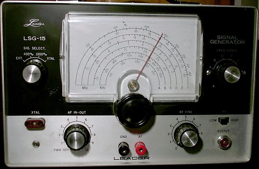
A signal generator is one of a class of electronic devices that generates electrical signals with set properties of amplitude, frequency, and wave shape. These generated signals are used as a stimulus for electronic measurements, typically used in designing, testing, troubleshooting, and repairing electronic or electroacoustic devices, though it often has artistic uses as well. There are many different types of signal generators with different purposes and applications and at varying levels of expense. These types include function generators, RF and microwave signal generators, pitch generators, arbitrary waveform generators, digital pattern generators, and frequency generators. In general, no device is suitable for all possible applications. A signal generator may be as simple as an oscillator with calibrated frequency and amplitude. More general-purpose signal generators allow control of all the characteristics of a signal. Modern general-purpose signal generators will have ... [...More Info...] [...Related Items...] OR: [Wikipedia] [Google] [Baidu] |
Radio Frequency
Radio frequency (RF) is the oscillation rate of an alternating electric current or voltage or of a magnetic, electric or electromagnetic field or mechanical system in the frequency range from around to around . This is roughly between the upper limit of audio frequencies and the lower limit of infrared frequencies; these are the frequencies at which energy from an oscillating current can radiate off a conductor into space as radio waves. Different sources specify different upper and lower bounds for the frequency range. Electric current Electric currents that oscillate at radio frequencies (RF currents) have special properties not shared by direct current or lower audio frequency alternating current, such as the 50 or 60 Hz current used in electrical power distribution. * Energy from RF currents in conductors can radiate into space as electromagnetic waves ( radio waves). This is the basis of radio technology. * RF current does not penetrate deeply into electrical c ... [...More Info...] [...Related Items...] OR: [Wikipedia] [Google] [Baidu] |
Vacuum Chamber
A vacuum chamber is a rigid enclosure from which air and other gases are removed by a vacuum pump. This results in a low-pressure environment within the chamber, commonly referred to as a vacuum. A vacuum environment allows researchers to conduct physical experiments or to test mechanical devices which must operate in outer space (for example) or for processes such as vacuum drying or vacuum coating. Chambers are typically made of metals which may or may not shield applied external magnetic fields depending on wall thickness, frequency, resistivity, and permeability of the material used. Only some materials are suitable for vacuum use. Chambers often have multiple ports, covered with vacuum flanges, to allow instruments or windows to be installed in the walls of the chamber. In low to medium-vacuum applications, these are sealed with elastomer o-rings. In higher vacuum applications, the flanges have knife edges machined onto them, which cut into a copper gasket when the flang ... [...More Info...] [...Related Items...] OR: [Wikipedia] [Google] [Baidu] |
Anisotropy
Anisotropy () is the property of a material which allows it to change or assume different properties in different directions, as opposed to isotropy. It can be defined as a difference, when measured along different axes, in a material's physical or mechanical properties (absorbance, refractive index, conductivity, tensile strength, etc.). An example of anisotropy is light coming through a polarizer. Another is wood, which is easier to split along its grain than across it. Fields of interest Computer graphics In the field of computer graphics, an anisotropic surface changes in appearance as it rotates about its geometric normal, as is the case with velvet. Anisotropic filtering (AF) is a method of enhancing the image quality of textures on surfaces that are far away and steeply angled with respect to the point of view. Older techniques, such as bilinear and trilinear filtering, do not take into account the angle a surface is viewed from, which can result in aliasing or bl ... [...More Info...] [...Related Items...] OR: [Wikipedia] [Google] [Baidu] |


