|
Cross Section (electronics)
In electronics, a cross section, cross-section, or microsection, is a prepared electronics sample that allows analysis at a plane that cuts through the sample. It is a destructive technique requiring that a portion of the sample be cut or ground away to expose the internal plane for analysis. They are commonly prepared for research, manufacturing quality assurance, supplier conformity, and failure analysis. Printed wiring boards (PWBs) and electronic components and their solder joints are common cross sectioned samples. The features of interest to be analyzed in cross section can be nanometer-scale metal and dielectric layers in semiconductors up to macroscopic features such as the amount of solder that has filled into a large, 0.125in (3.18mm) diameter plated through hole. Preparation Cross sections can be prepared by several methods typically chosen based on the scale of the feature of interest because the technique affects the smoothness of the final polish. Smoother polishes ... [...More Info...] [...Related Items...] OR: [Wikipedia] [Google] [Baidu] |
Electronics
The field of electronics is a branch of physics and electrical engineering that deals with the emission, behaviour and effects of electrons using electronic devices. Electronics uses active devices to control electron flow by amplification and rectification, which distinguishes it from classical electrical engineering, which only uses passive effects such as resistance, capacitance and inductance to control electric current flow. Electronics has hugely influenced the development of modern society. The central driving force behind the entire electronics industry is the semiconductor industry sector, which has annual sales of over $481 billion as of 2018. The largest industry sector is e-commerce, which generated over $29 trillion in 2017. History and development Electronics has hugely influenced the development of modern society. The identification of the electron in 1897, along with the subsequent invention of the vacuum tube which could amplify and rectify small ... [...More Info...] [...Related Items...] OR: [Wikipedia] [Google] [Baidu] |
Silicon Carbide
Silicon carbide (SiC), also known as carborundum (), is a hard chemical compound containing silicon and carbon. A semiconductor, it occurs in nature as the extremely rare mineral moissanite, but has been mass-produced as a powder and crystal since 1893 for use as an abrasive. Grains of silicon carbide can be bonded together by sintering to form very hard ceramics that are widely used in applications requiring high endurance, such as car brakes, car clutches and ceramic plates in bulletproof vests. Large single crystals of silicon carbide can be grown by the Lely method and they can be cut into gems known as synthetic moissanite. Electronic applications of silicon carbide such as light-emitting diodes (LEDs) and Cat's whisker detector, detectors in early radios were first demonstrated around 1907. SiC is used in semiconductor electronics devices that operate at high temperatures or high voltages, or both. Natural occurrence Naturally occurring moissanite is found in only minut ... [...More Info...] [...Related Items...] OR: [Wikipedia] [Google] [Baidu] |
Energy-dispersive X-ray Spectroscopy
Energy-dispersive X-ray spectroscopy (EDS, EDX, EDXS or XEDS), sometimes called energy dispersive X-ray analysis (EDXA or EDAX) or energy dispersive X-ray microanalysis (EDXMA), is an analytical technique used for the elemental analysis or chemical characterization of a sample. It relies on an interaction of some source of X-ray excitation and a sample. Its characterization capabilities are due in large part to the fundamental principle that each element has a unique atomic structure allowing a unique set of peaks on its electromagnetic emission spectrum (which is the main principle of spectroscopy). The peak positions are predicted by the Moseley's law with accuracy much better than experimental resolution of a typical EDX instrument. To stimulate the emission of characteristic X-rays from a specimen a beam of electrons is focused into the sample being studied. At rest, an atom within the sample contains ground state (or unexcited) electrons in discrete energy levels or electron ... [...More Info...] [...Related Items...] OR: [Wikipedia] [Google] [Baidu] |
Optical Microscope
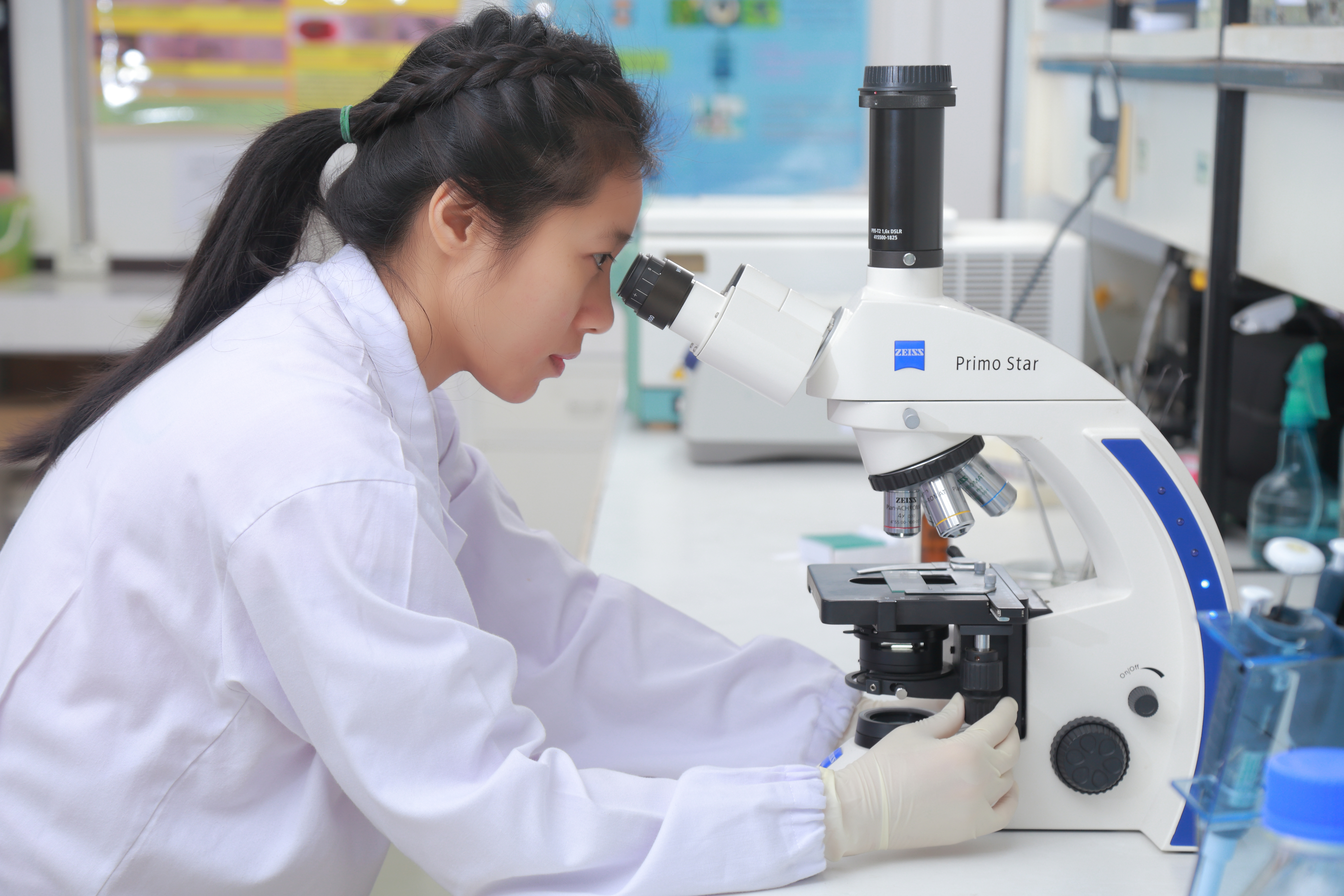
The optical microscope, also referred to as a light microscope, is a type of microscope that commonly uses visible light and a system of lenses to generate magnified images of small objects. Optical microscopes are the oldest design of microscope and were possibly invented in their present compound form in the 17th century. Basic optical microscopes can be very simple, although many complex designs aim to improve resolution and sample contrast. The object is placed on a stage and may be directly viewed through one or two eyepieces on the microscope. In high-power microscopes, both eyepieces typically show the same image, but with a stereo microscope, slightly different images are used to create a 3-D effect. A camera is typically used to capture the image (micrograph). The sample can be lit in a variety of ways. Transparent objects can be lit from below and solid objects can be lit with light coming through ( bright field) or around (dark field) the objective lens. Polarised ... [...More Info...] [...Related Items...] OR: [Wikipedia] [Google] [Baidu] |
Solder Fatigue
Solder fatigue is the mechanical degradation of solder due to deformation under cyclic loading. This can often occur at stress levels below the yield stress of solder as a result of repeated temperature fluctuations, mechanical vibrations, or mechanical loads. Techniques to evaluate solder fatigue behavior include finite element analysis and semi-analytical closed-form equations. Overview Solder is a metal alloy used to form electrical, thermal, and mechanical interconnections between the component and printed circuit board (PCB) substrate in an electronic assembly. Although other forms of cyclic loading are known to cause solder fatigue, it has been estimated that the largest portion of electronic failures are thermomechanically driven due to temperature cycling. Under thermal cycling, stresses are generated in the solder due to coefficient of thermal expansion (CTE) mismatches. This causes the solder joints to experience non-recoverable deformation via creep and plasticity tha ... [...More Info...] [...Related Items...] OR: [Wikipedia] [Google] [Baidu] |
Ion Milling Machine
An ion milling machine. Ion milling machine thins samples until they are transparent to electrons by firing ions (typically argon) at the surface from an angle and sputtering material from the surface. By making a sample electron transparent, it can be imaged and characterized in a transmission electron microscope (TEM). Ion beam milling may also be used for cross-section polishing prior to SEM analysis of materials that are difficult to prepare using mechanical polishing. See also * Focused ion beam * Transmission electron microscope Transmission electron microscopy (TEM) is a microscopy technique in which a beam of electrons is transmitted through a specimen to form an image. The specimen is most often an ultrathin section less than 100 nm thick or a suspension on a gr ... Electron microscopy {{sci-stub ... [...More Info...] [...Related Items...] OR: [Wikipedia] [Google] [Baidu] |
Focused Ion Beam
Focused ion beam, also known as FIB, is a technique used particularly in the semiconductor industry, materials science and increasingly in the biological field for site-specific analysis, deposition, and ablation of materials. A FIB setup is a scientific instrument that resembles a scanning electron microscope (SEM). However, while the SEM uses a focused beam of electrons to image the sample in the chamber, a FIB setup uses a focused beam of ions instead. FIB can also be incorporated in a system with both electron and ion beam columns, allowing the same feature to be investigated using either of the beams. FIB should not be confused with using a beam of focused ions for direct write lithography (such as in proton beam writing). These are generally quite different systems where the material is modified by other mechanisms. Ion beam source Most widespread instruments are using liquid metal ion sources (LMIS), especially gallium ion sources. Ion sources based on elemental gold an ... [...More Info...] [...Related Items...] OR: [Wikipedia] [Google] [Baidu] |
Diamond
Diamond is a Allotropes of carbon, solid form of the element carbon with its atoms arranged in a crystal structure called diamond cubic. Another solid form of carbon known as graphite is the Chemical stability, chemically stable form of carbon at Standard conditions for temperature and pressure, room temperature and pressure, but diamond is metastable and converts to it at a negligible rate under those conditions. Diamond has the highest Scratch hardness, hardness and thermal conductivity of any natural material, properties that are used in major industrial applications such as cutting and polishing tools. They are also the reason that diamond anvil cells can subject materials to pressures found deep in the Earth. Because the arrangement of atoms in diamond is extremely rigid, few types of impurity can contaminate it (two exceptions are boron and nitrogen). Small numbers of lattice defect, defects or impurities (about one per million of lattice atoms) color diamond blue (bor ... [...More Info...] [...Related Items...] OR: [Wikipedia] [Google] [Baidu] |
Epoxy
Epoxy is the family of basic components or cured end products of epoxy resins. Epoxy resins, also known as polyepoxides, are a class of reactive prepolymers and polymers which contain epoxide groups. The epoxide functional group is also collectively called ''epoxy''. The IUPAC name for an epoxide group is an oxirane. Epoxy resins may be reacted (cross-linked) either with themselves through catalytic homopolymerisation, or with a wide range of co-reactants including polyfunctional amines, acids (and acid anhydrides), phenols, alcohols and thiols (usually called mercaptans). These co-reactants are often referred to as hardeners or curatives, and the cross-linking reaction is commonly referred to as curing. Reaction of polyepoxides with themselves or with polyfunctional hardeners forms a thermosetting polymer, often with favorable mechanical properties and high thermal and chemical resistance. Epoxy has a wide range of applications, including metal coatings, composites, use in ... [...More Info...] [...Related Items...] OR: [Wikipedia] [Google] [Baidu] |
Quality Assurance
Quality assurance (QA) is the term used in both manufacturing and service industries to describe the systematic efforts taken to ensure that the product(s) delivered to customer(s) meet with the contractual and other agreed upon performance, design, reliability, and maintainability expectations of that customer. The core purpose of Quality Assurance is to prevent mistakes and defects in the development and production of both manufactured products, such as automobiles and shoes, and delivered services, such as automotive repair and athletic shoe design. Assuring quality and therefore avoiding problems and delays when delivering products or services to customers is what ISO 9000 defines as that "part of quality management focused on providing confidence that quality requirements will be fulfilled". This defect prevention aspect of quality assurance differs from the defect detection aspect of quality control and has been referred to as a ''shift left'' since it focuses on quality effor ... [...More Info...] [...Related Items...] OR: [Wikipedia] [Google] [Baidu] |
Ceramic Capacitor
A ceramic capacitor is a fixed-value capacitor where the ceramic material acts as the dielectric. It is constructed of two or more alternating layers of ceramic and a metal layer acting as the electrodes. The composition of the ceramic material defines the electrical behavior and therefore applications. Ceramic capacitors are divided into two application classes: * Class 1 ceramic capacitors offer high stability and low losses for resonant circuit applications. * Class 2 ceramic capacitors offer high volumetric efficiency for buffer, by-pass, and coupling applications. Ceramic capacitors, especially multilayer ceramic capacitors (MLCCs), are the most produced and used capacitors in electronic equipment that incorporate approximately one trillion (1012) pieces per year.Download Ceramic capacitors of special shapes and styles are ... [...More Info...] [...Related Items...] OR: [Wikipedia] [Google] [Baidu] |


