|
4D Scanning Transmission Electron Microscopy (4D STEM)
4D scanning transmission electron microscopy (4D STEM) is a subset of scanning transmission electron microscopy (STEM) which utilizes a pixelated electron detector to capture a convergent beam electron diffraction (CBED) pattern at each scan location. This technique captures a 2 dimensional reciprocal space image associated with each scan point as the beam rasters across a 2 dimensional region in real space, hence the name 4D STEM. Its development was enabled by evolution in STEM detectors and improvements in computational power. The technique has applications in visual diffraction imaging, phase orientation and strain mapping, phase contrast analysis, among others. The name 4D STEM is common in literature, however it is known by other names: 4D STEM EELS, ND STEM (N- since the number of dimensions could be higher than 4), position resolved diffraction (PRD), spatial resolved diffractometry, momentum-resolved STEM, "nanobeam precision electron diffraction", scanning electron nano di ... [...More Info...] [...Related Items...] OR: [Wikipedia] [Google] [Baidu] |
Scanning Transmission Electron Microscopy
A scanning transmission electron microscope (STEM) is a type of transmission electron microscope (TEM). Pronunciation is [stɛm] or [ɛsti:i:ɛm]. As with a conventional transmission electron microscope (CTEM), images are formed by electrons passing through a sufficiently thin specimen. However, unlike CTEM, in STEM the electron beam is focused to a fine spot (with the typical spot size 0.05 – 0.2 nm) which is then scanned over the sample in a raster illumination system constructed so that the sample is illuminated at each point with the beam parallel to the optical axis. The rastering of the beam across the sample makes STEM suitable for analytical techniques such as Z-contrast annular dark-field imaging, and spectroscopic mapping by energy-dispersive X-ray spectroscopy, energy dispersive X-ray (EDX) spectroscopy, or electron energy loss spectroscopy (EELS). These signals can be obtained simultaneously, allowing direct correlation of images and spectroscopic data. A ty ... [...More Info...] [...Related Items...] OR: [Wikipedia] [Google] [Baidu] |
HAADF
Annular dark-field imaging is a method of mapping samples in a scanning transmission electron microscope (STEM). These images are formed by collecting scattered electrons with an annular dark-field detector. Conventional TEM dark-field imaging uses an objective aperture to only collect scattered electrons that pass through. In contrast, STEM dark-field imaging does not use an aperture to differentiate the scattered electrons from the main beam, but uses an annular detector to collect only the scattered electrons. Consequently, the contrast mechanisms are different between conventional dark field imaging and the STEM dark field. An annular dark field detector collects electrons from an annulus around the beam, sampling far more scattered electrons than can pass through an objective aperture. This gives an advantage in terms of signal collection efficiency and allows the main beam to pass to an electron energy loss spectroscopy (EELS) detector, allowing both types of measurement ... [...More Info...] [...Related Items...] OR: [Wikipedia] [Google] [Baidu] |
Precession Electron Diffraction
Precession electron diffraction (PED) is a specialized method to collect electron diffraction patterns in a transmission electron microscope (TEM). By rotating (precessing) a tilted incident electron beam around the central axis of the microscope, a PED pattern is formed by integration over a collection of diffraction conditions. This produces a quasi-kinematical diffraction pattern that is more suitable as input into direct methods (crystallography), direct methods algorithms to determine the crystal structure of the sample. Overview Geometry Precession electron diffraction is accomplished utilizing the standard instrument configuration of a modern Transmission electron microscope, TEM. The animation illustrates the geometry used to generate a PED pattern. Specifically, the beam tilt coils located pre-specimen are used to tilt the electron beam off of the optic axis so it is incident with the specimen at an angle, φ. The image shift coils post-specimen are then used to til ... [...More Info...] [...Related Items...] OR: [Wikipedia] [Google] [Baidu] |
Kikuchi Lines (physics)
Kikuchi lines are patterns of electrons formed by scattering. They pair up to form bands in electron diffraction from single crystal specimens, there to serve as "roads in orientation-space" for microscopists uncertain of what they are looking at. In transmission electron microscopes, they are easily seen in diffraction from regions of the specimen thick enough for multiple scattering. Unlike diffraction spots, which blink on and off as one tilts the crystal, Kikuchi bands mark orientation space with well-defined intersections (called zones or poles) as well as paths connecting one intersection to the next. Experimental and theoretical maps of Kikuchi band geometry, as well as their direct-space analogs e.g. bend contours, electron channeling patterns, and fringe visibility maps are increasingly useful tools in electron microscopy of crystalline and nanocrystalline materials. Because each Kikuchi line is associated with Bragg diffraction from one side of a single set of lattice pl ... [...More Info...] [...Related Items...] OR: [Wikipedia] [Google] [Baidu] |
Transmission Electron Microscopy
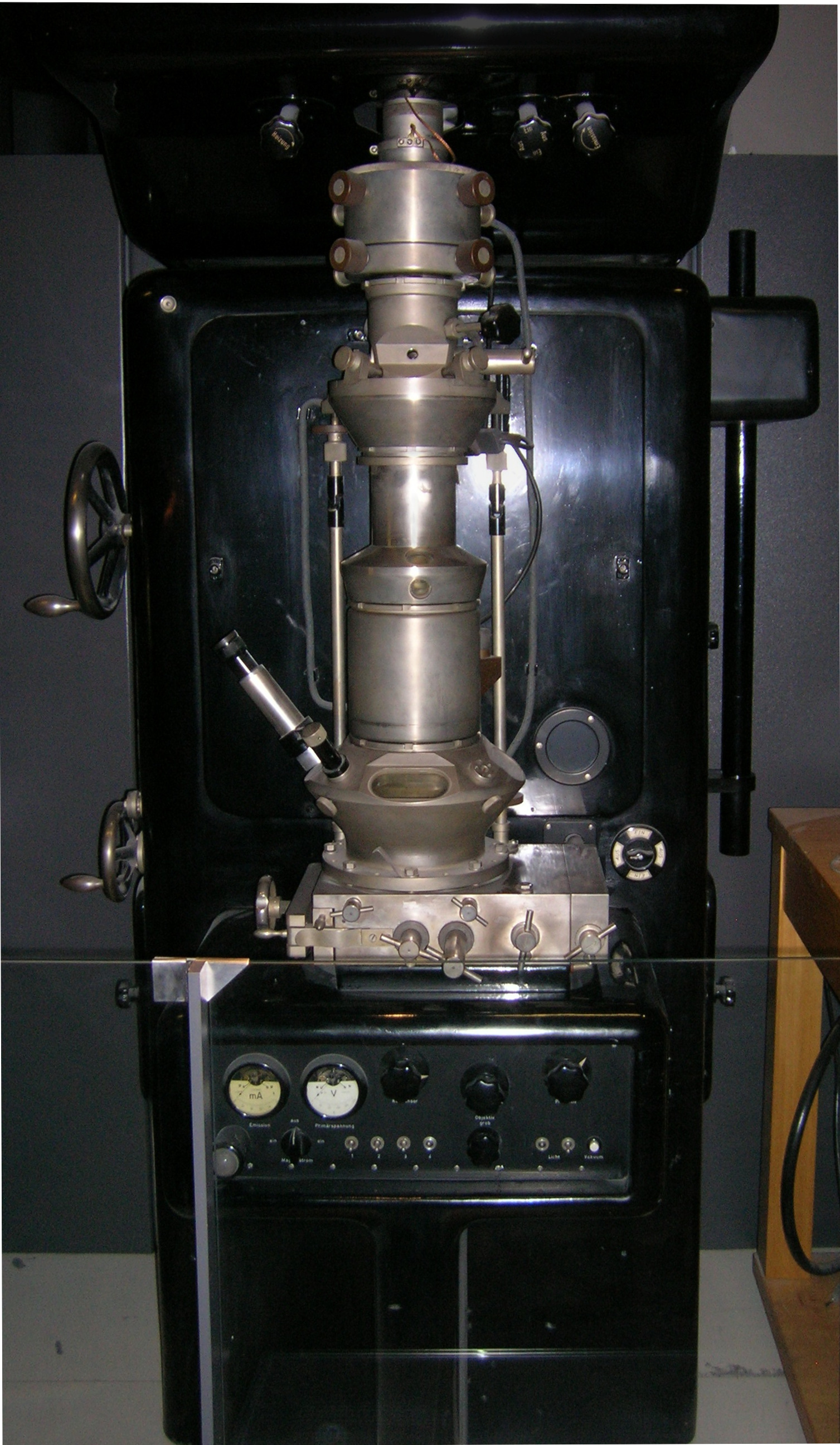
Transmission electron microscopy (TEM) is a microscopy technique in which a beam of electrons is transmitted through a specimen to form an image. The specimen is most often an ultrathin section less than 100 nm thick or a suspension on a grid. An image is formed from the interaction of the electrons with the sample as the beam is transmitted through the specimen. The image is then magnified and focused onto an imaging device, such as a fluorescent screen, a layer of photographic film, or a detector such as a scintillator attached to a charge-coupled device or a direct electron detector. Transmission electron microscopes are capable of imaging at a significantly higher resolution than light microscopes, owing to the smaller de Broglie wavelength of electrons. This enables the instrument to capture fine detail—even as small as a single column of atoms, which is thousands of times smaller than a resolvable object seen in a light microscope. Transmission electron micr ... [...More Info...] [...Related Items...] OR: [Wikipedia] [Google] [Baidu] |
Scanning Electron Microscope
A scanning electron microscope (SEM) is a type of electron microscope that produces images of a sample by scanning the surface with a focused beam of electrons. The electrons interact with atoms in the sample, producing various signals that contain information about the surface topography and composition. The electron beam is scanned in a raster scan pattern, and the position of the beam is combined with the intensity of the detected signal to produce an image. In the most common SEM mode, secondary electrons emitted by atoms excited by the electron beam are detected using a secondary electron detector ( Everhart–Thornley detector). The number of secondary electrons that can be detected, and thus the signal intensity, depends, among other things, on specimen topography. Some SEMs can achieve resolutions better than 1 nanometer. Specimens are observed in high vacuum in a conventional SEM, or in low vacuum or wet conditions in a variable pressure or environmental SEM, an ... [...More Info...] [...Related Items...] OR: [Wikipedia] [Google] [Baidu] |
Metal–organic Framework
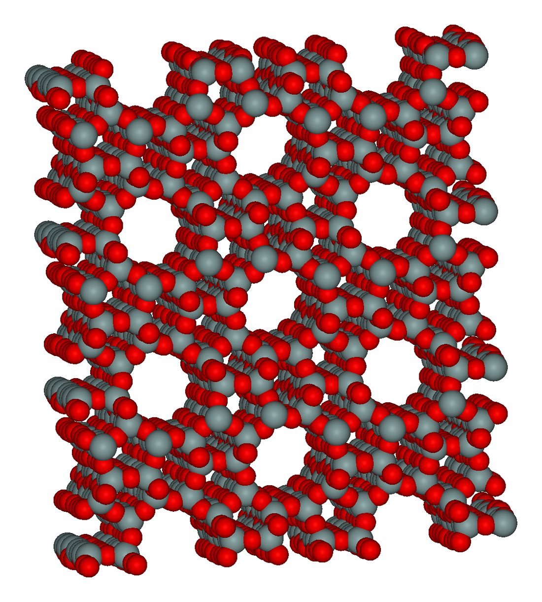
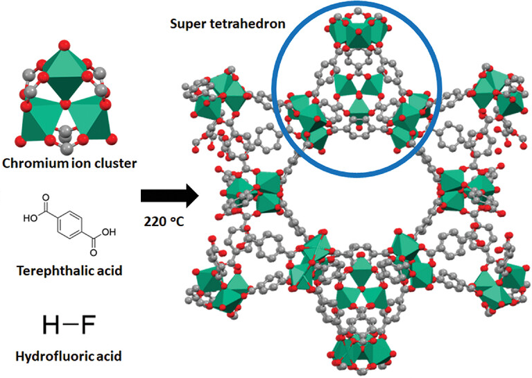
Metal–organic frameworks (MOFs) are a class of porous polymers consisting of metal cluster compound, clusters (also known as Secondary Building Units - SBUs) coordinated to organic compound, organic ligands to form one-, two- or three-dimensional structures. The organic ligands included are sometimes referred to as "struts" or "linkers", one example being terephthalic acid, 1,4-benzenedicarboxylic acid (BDC). MOFs are classified as reticular materials. More formally, a metal–organic framework is a potentially porous extended structure made from metal ions and organic linkers. An extended structure is a structure whose sub-units occur in a constant ratio and are arranged in a repeating pattern. MOFs are a subclass of coordination networks, which is a coordination compound extending, through repeating coordination entities, in one dimension, but with cross-links between two or more individual chains, loops, or spiro-links, or a coordination compound extending through repeating c ... [...More Info...] [...Related Items...] OR: [Wikipedia] [Google] [Baidu] |
Strain Mapping
Strain may refer to: Science and technology * Strain (biology), variants of biological organisms * Strain (chemistry), a chemical stress of a molecule * Strain (general relativity), measure of spacetime stretching in linearized gravity * Strain (injury), an injury to a muscle * Strain (mechanics), a measure of deformation * Filtration, separating fluids from solids by passing through a filter * Percolation, of fluids through porous materials * Psychological stress Other uses * straining, in cooking, by a strainer or sieve. * Strain, a term in contract bridge Proper names * Strain (surname) Arts and media * ''Strain'' (manga), 1996 * Strain (music), phrases of a piece * ''Strain'' (album), 2004, by Flesh Field * '' Strain: Strategic Armored Infantry'', a 2006 anime * ''Strain'' (film), a 2020 Nigerian drama Places * Strain, Arkansas, US, an unincorporated community * Strain, Missouri, US, an unincorporated community See also * Overwork * S Train (other) * S ... [...More Info...] [...Related Items...] OR: [Wikipedia] [Google] [Baidu] |
Phase Orientation Mapping
Phase or phases may refer to: Science *State of matter, or phase, one of the distinct forms in which matter can exist *Phase (matter), a region of space throughout which all physical properties are essentially uniform *Phase space, a mathematical space in which each possible state of a physical system is represented by a point also referred to as a "microscopic state" **Phase space formulation, a formulation of quantum mechanics in phase space *Phase (waves), the position of a point in time (an instant) on a waveform cycle **Instantaneous phase, generalization for both cyclic and non-cyclic phenomena *AC phase, the phase offset between alternating current electric power in multiple conducting wires **Single-phase electric power, distribution of AC electric power in a system where the voltages of the supply vary in unison **Three-phase electric power, a common method of AC electric power generation, transmission, and distribution *Phase problem, the loss of information (the phase) ... [...More Info...] [...Related Items...] OR: [Wikipedia] [Google] [Baidu] |
Diffraction Pattern
Diffraction is the deviation of waves from straight-line propagation without any change in their energy due to an obstacle or through an aperture. The diffracting object or aperture effectively becomes a secondary source of the propagating wave. Diffraction is the same physical effect as interference, but interference is typically applied to superposition of a few waves and the term diffraction is used when many waves are superposed. Italian scientist Francesco Maria Grimaldi coined the word ''diffraction'' and was the first to record accurate observations of the phenomenon in 1660. In classical physics, the diffraction phenomenon is described by the Huygens–Fresnel principle that treats each point in a propagating wavefront as a collection of individual spherical wavelets. The characteristic pattern is most pronounced when a wave from a coherent source (such as a laser) encounters a slit/aperture that is comparable in size to its wavelength, as shown in the inserted image. ... [...More Info...] [...Related Items...] OR: [Wikipedia] [Google] [Baidu] |
Dark-field Microscopy
Dark-field microscopy, also called dark-ground microscopy, describes microscopy methods, in both light and electron microscopy, which exclude the unscattered beam from the image. Consequently, the field around the specimen (i.e., where there is no specimen to scatter the beam) is generally dark. In optical microscopes a darkfield condenser lens must be used, which directs a cone of light away from the objective lens. To maximize the scattered light-gathering power of the objective lens, oil immersion is used and the numerical aperture (NA) of the objective lens must be less than 1.0. Objective lenses with a higher NA can be used but only if they have an adjustable diaphragm, which reduces the NA. Often these objective lenses have a NA that is variable from 0.7 to 1.25. Light microscopy applications In optical microscopy, dark-field describes an illumination technique used to enhance the contrast in unstained samples. It works by illuminating the sample with light that wil ... [...More Info...] [...Related Items...] OR: [Wikipedia] [Google] [Baidu] |
Virtual Diffraction Imaging In 4D STEM
Virtual may refer to: * Virtual image, an apparent image of an object (as opposed to a real object), in the study of optics * Virtual (horse), a thoroughbred racehorse * Virtual channel, a channel designation which differs from that of the actual radio channel (or range of frequencies) on which the signal travels * Virtual function, a programming function or method whose behaviour can be overridden within an inheriting class by a function with the same signature * Virtual machine, the virtualization of a computer system * Virtual meeting, or web conferencing * Virtual memory, a memory management technique that abstracts the memory address space in a computer * Virtual particle, a type of short-lived particle of indeterminate mass * Virtual reality (virtuality), computer programs with an interface that gives the user the impression that they are physically inside a simulated space * Virtual world, a computer-based simulated environment populated by many users who can create a persona ... [...More Info...] [...Related Items...] OR: [Wikipedia] [Google] [Baidu] |


