|
2DEG
A two-dimensional electron gas (2DEG) is a scientific model in solid-state physics. It is an electron gas that is free to move in two dimensions, but tightly confined in the third. This tight confinement leads to quantized energy levels for motion in the third direction, which can then be ignored for most problems. Thus the electrons appear to be a 2D sheet embedded in a 3D world. The analogous construct of holes is called a two-dimensional hole gas (2DHG), and such systems have many useful and interesting properties. Realizations Most 2DEGs are found in transistor-like structures made from semiconductors. The most commonly encountered 2DEG is the layer of electrons found in MOSFETs (metal-oxide-semiconductor field-effect transistors). When the transistor is in inversion mode, the electrons underneath the gate oxide are confined to the semiconductor-oxide interface, and thus occupy well defined energy levels. For thin-enough potential wells and temperatures not too high, onl ... [...More Info...] [...Related Items...] OR: [Wikipedia] [Google] [Baidu] |
Lanthanum Aluminate-strontium Titanate Interface
The interface between lanthanum aluminate (LaAlO3) and strontium titanate (SrTiO3) is a notable materials interface because it exhibits properties not found in its constituent materials. Individually, LaAlO3 and SrTiO3 are non-magnetic insulators, yet LaAlO3/SrTiO3 interfaces can exhibit electrical metallic conductivity, superconductivity, ferromagnetism, large negative in-plane magnetoresistance, and giant persistent photoconductivity. The study of how these properties emerge at the LaAlO3/SrTiO3 interface is a growing area of research in condensed matter physics. Emergent properties Conductivity Under the right conditions, the LaAlO3/SrTiO3 interface is electrically conductive, like a metal. The angular dependence of Shubnikov–de Haas oscillations indicates that the conductivity is two-dimensional, leading many researchers to refer to it as a two-dimensional electron gas (2DEG). Two-dimensional does not mean that the conductivity has zero thickness, but rather that th ... [...More Info...] [...Related Items...] OR: [Wikipedia] [Google] [Baidu] |
HEMT
A high-electron-mobility transistor (HEMT), also known as heterostructure FET (HFET) or modulation-doped FET (MODFET), is a field-effect transistor incorporating a junction between two materials with different band gaps (i.e. a heterojunction) as the channel instead of a doped region (as is generally the case for a MOSFET). A commonly used material combination is GaAs with AlGaAs, though there is wide variation, dependent on the application of the device. Devices incorporating more indium generally show better high-frequency performance, while in recent years, gallium nitride HEMTs have attracted attention due to their high-power performance. Like other FETs, HEMTs are used in integrated circuits as digital on-off switches. FETs can also be used as amplifiers for large amounts of current using a small voltage as a control signal. Both of these uses are made possible by the FET’s unique current–voltage characteristics. HEMT transistors are able to operate at higher frequenc ... [...More Info...] [...Related Items...] OR: [Wikipedia] [Google] [Baidu] |
Electron Mobility
In solid-state physics, the electron mobility characterises how quickly an electron can move through a metal or semiconductor when pulled by an electric field. There is an analogous quantity for holes, called hole mobility. The term carrier mobility refers in general to both electron and hole mobility. Electron and hole mobility are special cases of electrical mobility of charged particles in a fluid under an applied electric field. When an electric field ''E'' is applied across a piece of material, the electrons respond by moving with an average velocity called the drift velocity, v_d. Then the electron mobility ''μ'' is defined as v_d = \mu E. Electron mobility is almost always specified in units of cm2/( V⋅ s). This is different from the SI unit of mobility, m2/( V⋅ s). They are related by 1 m2/(V⋅s) = 104 cm2/(V⋅s). Conductivity is proportional to the product of mobility and carrier concentration. For example, the same conductivity could come from a small n ... [...More Info...] [...Related Items...] OR: [Wikipedia] [Google] [Baidu] |
Quantum Well
A quantum well is a potential well with only discrete energy values. The classic model used to demonstrate a quantum well is to confine particles, which were initially free to move in three dimensions, to two dimensions, by forcing them to occupy a planar region. The effects of quantum confinement take place when the quantum well thickness becomes comparable to the de Broglie wavelength of the carriers (generally electrons and holes), leading to energy levels called "energy subbands", i.e., the carriers can only have discrete energy values. A wide variety of electronic quantum well devices have been developed based on the theory of quantum well systems. These devices have found applications in lasers, photodetectors, modulators, and switches for example. Compared to conventional devices, quantum well devices are much faster and operate much more economically and are a point of incredible importance to the technological and telecommunication industries. These quantum well devic ... [...More Info...] [...Related Items...] OR: [Wikipedia] [Google] [Baidu] |
Heterojunction
A heterojunction is an interface between two layers or regions of dissimilar semiconductors. These semiconducting materials have unequal band gaps as opposed to a homojunction. It is often advantageous to engineer the electronic energy bands in many solid-state device applications, including semiconductor lasers, solar cells and transistors. The combination of multiple heterojunctions together in a device is called a heterostructure, although the two terms are commonly used interchangeably. The requirement that each material be a semiconductor with unequal band gaps is somewhat loose, especially on small length scales, where electronic properties depend on spatial properties. A more modern definition of heterojunction is the interface between any two solid-state materials, including crystalline and amorphous structures of metallic, insulating, fast ion conductor and semiconducting materials. Manufacture and applications Heterojunction manufacturing generally requires the use of ... [...More Info...] [...Related Items...] OR: [Wikipedia] [Google] [Baidu] |
Topological Insulator
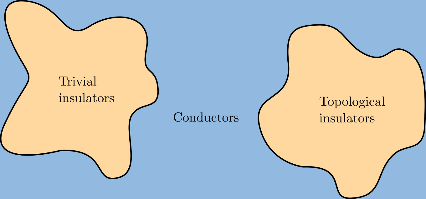
A topological insulator is a material whose interior behaves as an electrical insulator while its surface behaves as an electrical conductor, meaning that electrons can only move along the surface of the material. A topological insulator is an insulator for the same reason a " trivial" (ordinary) insulator is: there exists an energy gap between the valence and conduction bands of the material. But in a topological insulator, these bands are, in an informal sense, "twisted", relative to a trivial insulator. The topological insulator cannot be continuously transformed into a trivial one without untwisting the bands, which closes the band gap and creates a conducting state. Thus, due to the continuity of the underlying field, the border of a topological insulator with a trivial insulator (including vacuum, which is topologically trivial) is forced to support a conducting state. Since this results from a global property of the topological insulator's band structure, local (sym ... [...More Info...] [...Related Items...] OR: [Wikipedia] [Google] [Baidu] |
FET Cross Section
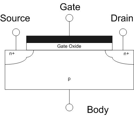
The field-effect transistor (FET) is a type of transistor that uses an electric field to control the flow of current in a semiconductor. FETs ( JFETs or MOSFETs) are devices with three terminals: ''source'', ''gate'', and ''drain''. FETs control the flow of current by the application of a voltage to the gate, which in turn alters the conductivity between the drain and source. FETs are also known as unipolar transistors since they involve single-carrier-type operation. That is, FETs use either electrons (n-channel) or holes (p-channel) as charge carriers in their operation, but not both. Many different types of field effect transistors exist. Field effect transistors generally display very high input impedance at low frequencies. The most widely used field-effect transistor is the MOSFET (metal-oxide-semiconductor field-effect transistor). History The concept of a field-effect transistor (FET) was first patented by Austro-Hungarian physicist Julius Edgar Lilienfeld in 192 ... [...More Info...] [...Related Items...] OR: [Wikipedia] [Google] [Baidu] |
Ionized Impurity Scattering
In quantum mechanics, ionized impurity scattering is the scattering of charge carriers by ionization in the lattice. The most primitive models can be conceptually understood as a particle responding to unbalanced local charge that arises near a crystal impurity; similar to an electron encountering an electric field. This effect is the mechanism by which doping decreases mobility. In the current quantum mechanical picture of conductivity the ease with which electrons traverse a crystal lattice is dependent on the near perfectly regular spacing of ions in that lattice. Only when a lattice contains perfectly regular spacing can the ion-lattice interaction (scattering) lead to almost transparent behavior of the lattice. Impurity atoms in a crystal have an effect similar to thermal vibrations where conductivity has a direct relationship between temperature. A crystal with impurities is less regular than a pure crystal, and a reduction in electron mean free paths occurs. Impure crystals h ... [...More Info...] [...Related Items...] OR: [Wikipedia] [Google] [Baidu] |
Nature Materials
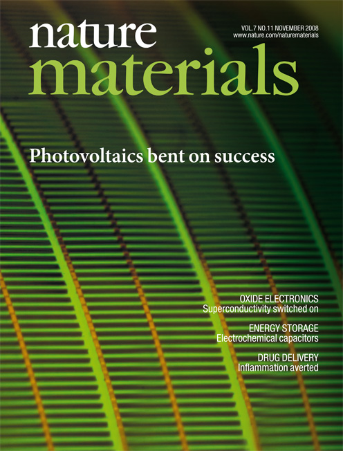
''Nature Materials'', is a peer-reviewed scientific journal published by Nature Publishing Group. It was launched in September 2002. Vincent Dusastre is the launching and current chief editor. Aims and scope ''Nature Materials'' is focused on all topics within the combined disciplines of '' materials science'' and ''engineering''. Topics published in the journal are presented from the view of the impact that materials research has on other scientific disciplines such as (for example) physics, chemistry, and biology. Coverage in this journal encompasses fundamental research and applications from synthesis to processing, and from structure to composition. Coverage also includes basic research and applications of properties and performance of materials. Materials are specifically described as "substances in the condensed states (liquid, solid, colloidal)", and which are "designed or manipulated for technological ends." Furthermore, ''Nature Materials'' functions as a forum for th ... [...More Info...] [...Related Items...] OR: [Wikipedia] [Google] [Baidu] |
Physical Review B
''Physical Review B: Condensed Matter and Materials Physics'' (also known as PRB) is a peer-reviewed, scientific journal, published by the American Physical Society (APS). The Editor of PRB is Laurens W. Molenkamp. It is part of the ''Physical Review'' family of journals. About the Physical Review Journals The current Editor in Chief is Michael Thoennessen. PRB currently publishes over 4500 papers a year, making it one of the largest physics journals in the world. PRB ranked by the Eigenfactor, University of Washington, 2012 Scop ...
|
Nature (journal)
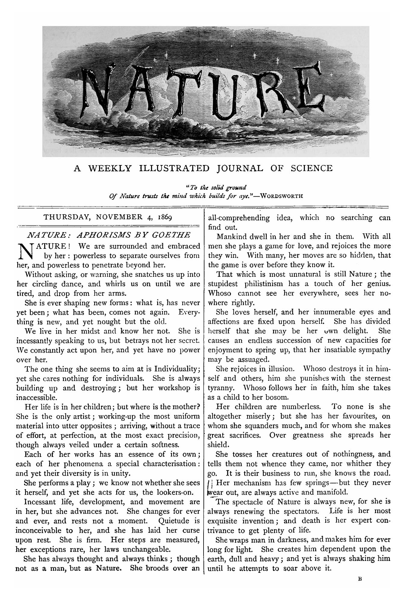
''Nature'' is a British weekly scientific journal founded and based in London, England. As a multidisciplinary publication, ''Nature'' features peer-reviewed research from a variety of academic disciplines, mainly in science and technology. It has core editorial offices across the United States, continental Europe, and Asia under the international scientific publishing company Springer Nature. ''Nature'' was one of the world's most cited scientific journals by the Science Edition of the 2019 '' Journal Citation Reports'' (with an ascribed impact factor of 42.778), making it one of the world's most-read and most prestigious academic journals. , it claimed an online readership of about three million unique readers per month. Founded in autumn 1869, ''Nature'' was first circulated by Norman Lockyer and Alexander Macmillan as a public forum for scientific innovations. The mid-20th century facilitated an editorial expansion for the journal; ''Nature'' redoubled its efforts in ... [...More Info...] [...Related Items...] OR: [Wikipedia] [Google] [Baidu] |


