Time-interleaved ADC on:
[Wikipedia]
[Google]
[Amazon]
Time interleaved (TI) ADCs are Analog-to-Digital Converters (ADCs) that involve ''M'' converters working in parallel. Each of the ''M'' converters is referred to as sub-ADC, channel or slice in the literature. The time interleaving technique, akin to multithreading in computing, involves using multiple converters in parallel to sample the input signal at staggered intervals, increasing the overall sampling rate and improving performance without overburdening the single ADCs.
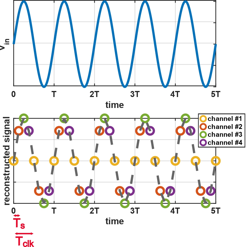
 In a time-interleaved system, the conversion time required by each sub-ADC is equal to . If the outputs of the multiple channels are properly combined, the overall system can be considered as a single converter operating at a sampling period equal to , where represents the number of channels or sub-ADCs in the TI system.
To illustrate this concept, let us delve into the conversion process of a TI ADC with reference to the first figure of this paragraph. The figure shows the time diagram of a data converter that employs four interleaved channels. The input signal (depicted as a blue waveform) is a sinusoidal wave at frequency . Here, is the clock frequency, which is the reciprocal of , the overall sampling period of the TI ADC. This relationship aligns with the Shannon-Nyquist sampling theorem, which states that the sampling rate must be at least twice the highest frequency present in the input signal to accurately reconstruct the signal without aliasing.
In a TI ADC, every , one of the channels acquires a sample of the input signal. The conversion operation performed by each sub-ADC takes seconds and, after the conversion, a digital multiplexer sequentially selects the output from one of the sub-ADCs. This selection occurs in a specific order, typically from the first sub-ADC to the sub-ADC, and then the cycle repeats.
At any given moment, each channel is engaged in converting different samples. Consequently, the aggregate data rate of the system is faster than the data rate of a single sub-ADC by a factor of . This is because the TI system essentially parallelizes the conversion process across multiple sub-ADCs. The factor , representing the number of interleaved channels, thus represents the increase in the overall sampling rate of the entire system.
To conclude, the time-interleaving method effectively increases the conversion speed of each sub-ADC by times. As a result, even though each sub-ADC operates at a relatively slow pace, the combined output of the TI system is characterized by a higher sampling rate. Time interleaving is therefore a powerful technique in the design and implementation of data converters since it enables the creation of high-speed ADCs using components that individually have much lower performance capabilities in terms of speed.
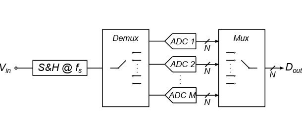
 Two architectures are possible to implement a time interleaved ADC. The first architecture is depicted in the first figure of the paragraph and it is characterized by the presence of a single Sample and Hold (S&H) circuit for the entire structure. The sampler operates at a frequency and acquires the samples for all the channels of the TI ADC. Once a sample is acquired, an analog demultiplexer distributes it to the correspondent sub-ADC. This approach centralizes the sampling process, ensuring uniformity in the acquired samples. However, it places stringent speed requirements on the S&H circuit since it must operate at the full sampling rate of the ADC system.
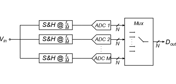
In contrast, the second architecture, illustrated in the second figure of the paragraph, employs different S&H circuits for each channel, each operating at a reduced frequency , where is once again the number of interleaved channels. This solution significantly relaxes the speed requirements for each S&H circuit, as they only need to operate at a fraction of the overall sampling rate. This approach mitigates the challenge of high-speed operation of the first architecture. However, this benefit comes with trade-offs, namely, increased area occupation and higher power dissipation due to the additional circuitry required to implement multiple S&H circuits.
 A receiver is one of the essential components of a
History
Early concept
The concept of time interleaving can be traced back to the 1960s. One of the earliest mentions of using multiple ADCs to increase sampling rates appeared in the work of Bernard M. Oliver andClaude E. Shannon
Claude Elwood Shannon (April 30, 1916 – February 24, 2001) was an American mathematician, electrical engineer, computer scientist, cryptographer and inventor known as the "father of information theory" and the man who laid the foundations of th ...
. Their pioneering work on communication theory and sampling laid the groundwork for the theoretical basis of time interleaving. However, practical implementations were limited by the technology of the time.
Development
In the 1980s, significant advancements were made: W. C. Black and D. A. Hodges from the Berkeley University successfully implemented the first prototype of a time interleaved ADC. In particular, they designed a 4-way interleaved converter working at 2.5 MSample/s. Each slice of the converter was a 7-stage SAR pipeline ADC running at 625 kSample/s. Aneffective number of bits
Effective number of bits (ENOB) is a measure of the real dynamic range of an analog-to-digital converter (ADC), digital-to-analog converter (DAC), or associated circuitry. Although the resolution of a converter may be specified by the number of b ...
(ENOB) equal to 6.2 was measured for the proposed converter with a probing input signal at 100 kHz. The work was presented at ISSCC
International Solid-State Circuits Conference is a global forum for presentation of advances in solid-state circuits and Systems-on-a-Chip. The conference is held every year in February at the San Francisco Marriott Marquis in downtown San Fr ...
1980 and the paper was focused on the practical challenges of implementing TI ADCs, including the synchronization and calibration of multiple channels to reduce mismatches.
In 1987, Ken Poulton and other researchers of the HP Labs
HP Labs is the exploratory and advanced research group for HP Inc. HP Labs' headquarters is in Palo Alto, California and the group has research and development facilities in Bristol, UK. The development of programmable desktop calculators, ink ...
developed the first product based on Time Interleaved ADCs: the HP 54111D digital oscilloscope.
Commercialization
In the 1990s, the TI ADC technology saw further advancements driven by the increasing demand for high-speed data conversion in telecommunications and other fields. A notable project during this period was the development of high-speed ADCs for digital oscilloscopes byTektronix
Tektronix, Inc., historically widely known as Tek, is an American company best known for manufacturing test and measurement devices such as oscilloscopes, logic analyzers, and video and mobile test protocol equipment. Originally an independent c ...
. Engineers at Tektronix implemented TI ADCs to achieve the high sampling rates necessary for capturing fast transient signals in test and measurement equipment. As a result of this work, the Tektronix TDS350, a two-channel, 200 MHz, 1 GSample/s digital storage scope, was commercialized in 1991.
Widespread adoption
By the late 1990s, TI ADCs had become commercially viable. One of the key projects that showcased the potential of TI ADCs was the development of the GSM (Global System for Mobile Communications) standard, where high-speed ADCs were essential for digital signal processing in mobile phones. Companies likeAnalog Devices
Analog Devices, Inc. (ADI), also known simply as Analog, is an American multinational corporation, multinational semiconductor company specializing in data conversion, signal processing, and power management technology, headquartered in Wilming ...
and Texas Instruments
Texas Instruments Incorporated (TI) is an American multinational semiconductor company headquartered in Dallas, Texas. It is one of the top 10 semiconductor companies worldwide based on sales volume. The company's focus is on developing analog ...
began to offer TI ADCs as standard products, enabling widespread adoption in various applications.
Nowadays
The 21st century has seen continued innovation in TI ADC technology. Researchers and engineers have focused on further improving the performance and integration of TI ADCs to meet the growing demands of digital systems. Key figures in this era include Boris Murmann and his colleagues atStanford University
Leland Stanford Junior University, commonly referred to as Stanford University, is a Private university, private research university in Stanford, California, United States. It was founded in 1885 by railroad magnate Leland Stanford (the eighth ...
, who have contributed to the development of advanced calibration techniques and low-power design methods for TI ADCs.
Future perspectives
Today, TI ADCs are used in a wide range of applications, from 5G telecommunications to high-resolution medical imaging. The future of TI ADCs looks promising, with ongoing research focusing on further improving their performance and expanding their application areas. Emerging technologies such asautonomous vehicles
Vehicular automation is using technology to assist or replace the operator of a vehicle such as a car, truck, aircraft, rocket, military vehicle, or boat. Assisted vehicles are ''semi-autonomous'', whereas vehicles that can travel without a ...
, advanced radar systems, and artificial intelligence
Artificial intelligence (AI) is the capability of computer, computational systems to perform tasks typically associated with human intelligence, such as learning, reasoning, problem-solving, perception, and decision-making. It is a field of re ...
-driven signal processing will continue to drive the demand for high-speed, high-resolution ADCs.
Working principle

 In a time-interleaved system, the conversion time required by each sub-ADC is equal to . If the outputs of the multiple channels are properly combined, the overall system can be considered as a single converter operating at a sampling period equal to , where represents the number of channels or sub-ADCs in the TI system.
To illustrate this concept, let us delve into the conversion process of a TI ADC with reference to the first figure of this paragraph. The figure shows the time diagram of a data converter that employs four interleaved channels. The input signal (depicted as a blue waveform) is a sinusoidal wave at frequency . Here, is the clock frequency, which is the reciprocal of , the overall sampling period of the TI ADC. This relationship aligns with the Shannon-Nyquist sampling theorem, which states that the sampling rate must be at least twice the highest frequency present in the input signal to accurately reconstruct the signal without aliasing.
In a TI ADC, every , one of the channels acquires a sample of the input signal. The conversion operation performed by each sub-ADC takes seconds and, after the conversion, a digital multiplexer sequentially selects the output from one of the sub-ADCs. This selection occurs in a specific order, typically from the first sub-ADC to the sub-ADC, and then the cycle repeats.
At any given moment, each channel is engaged in converting different samples. Consequently, the aggregate data rate of the system is faster than the data rate of a single sub-ADC by a factor of . This is because the TI system essentially parallelizes the conversion process across multiple sub-ADCs. The factor , representing the number of interleaved channels, thus represents the increase in the overall sampling rate of the entire system.
To conclude, the time-interleaving method effectively increases the conversion speed of each sub-ADC by times. As a result, even though each sub-ADC operates at a relatively slow pace, the combined output of the TI system is characterized by a higher sampling rate. Time interleaving is therefore a powerful technique in the design and implementation of data converters since it enables the creation of high-speed ADCs using components that individually have much lower performance capabilities in terms of speed.
Possible architectures

 Two architectures are possible to implement a time interleaved ADC. The first architecture is depicted in the first figure of the paragraph and it is characterized by the presence of a single Sample and Hold (S&H) circuit for the entire structure. The sampler operates at a frequency and acquires the samples for all the channels of the TI ADC. Once a sample is acquired, an analog demultiplexer distributes it to the correspondent sub-ADC. This approach centralizes the sampling process, ensuring uniformity in the acquired samples. However, it places stringent speed requirements on the S&H circuit since it must operate at the full sampling rate of the ADC system.
In contrast, the second architecture, illustrated in the second figure of the paragraph, employs different S&H circuits for each channel, each operating at a reduced frequency , where is once again the number of interleaved channels. This solution significantly relaxes the speed requirements for each S&H circuit, as they only need to operate at a fraction of the overall sampling rate. This approach mitigates the challenge of high-speed operation of the first architecture. However, this benefit comes with trade-offs, namely, increased area occupation and higher power dissipation due to the additional circuitry required to implement multiple S&H circuits.
Advantages and trade-offs of the two architectures
The choice between these two architectures depends on the specific requirements and constraints of the application. The single S&H circuit architecture offers a compact and potentially lower-power solution, as it eliminates the redundancy of multiple S&H circuits. The centralized sampling can also reduce mismatches between channels, as all samples are derived from a single source. However, the high-speed requirement of the single S&H circuit can be a significant challenge, particularly at very high sampling rates where achieving the necessary performance may require more advanced and costly technology. On the other hand, the multiple S&H circuit architecture distributes the sampling load, allowing each S&H circuit to operate at a lower speed. This can be advantageous in applications where high-speed circuits are difficult or expensive to implement. Additionally, this architecture can offer improved flexibility in managing timing and gain mismatches between channels. Each S&H circuit can be independently optimized for its specific operating conditions, potentially leading to better overall performance. The trade-offs include a larger footprint on the integrated circuit and increased power consumption, which may be critical factors in power-sensitive or space-constrained applications. In practical implementations, the choice between these architectures is influenced by several factors, including the required sampling rate, power budget, available silicon area, and the acceptable level of complexity in calibration and error correction. For instance, in high-speed communication systems the single S&H circuit architecture might be preferred despite its stringent speed requirements, due to its compact design and potentially lower power consumption. Conversely, in applications where power is less of a concern but achieving ultra-high speeds is challenging, the multiple S&H circuit architecture might be more suitable.Sources of errors
Ideally, all the sub-ADCs are identical. In practice, however, they end up being slightly different due to process, voltage and temperature (PVT) variations. If not taken care of, sub-ADC mismatches can jeopardize the performance of TI ADCs since they show up in the output spectrum as spectral tones. Offset mismatches (i.e., different input-referred offsets for each sub-ADC) are superimposed to the converted signal as a sequence of period , affecting the output spectrum of the ADC with spurious tones, whose power depends on the magnitude of the offsets, located at frequencies , where M represents the number of channels and k is an arbitrary integer number from to . Gain errors affect the amplitude of the converted signal and are transferred to the output as an amplitude modulation (AM) of the input signal with a sequence of period . As a matter of fact, this mechanism introduces spurious harmonics at frequencies , whose power depends both on the amplitude of the input signal and on the magnitude of the gain error sequence. Finally, skew mismatches are due to the channels being timed by different phases of the same clock signal. If one timing signal is skewed with respect to the others, spurious harmonics will be generated in the output spectrum. It can be demonstrated that these spurs are located at the frequencies . Moreover, their power depends both on the magnitude of the skew between the control phases and on the value of the input signal frequency. Channel mismatches in a TI ADC can seriously degrade its Spurious-Free Dynamic Range (SFDR) and its Signal-to-Noise-and-Distortion Ratio (SNDR). To recover the spectral purity of the converter, the proven solution consists of compensating these non-idealities with digitally implemented corrections. Despite being able to recover the overall spectral purity by suppressing the mismatch spurs, digital calibrations can significantly increase the overall power consumption of the receiver and may not be as effective when the input signal is broadband. For this reason, methods to provide higher stability and usability in real-world cases should be actively researched.Typical applications
Telecommunications
As cellular communications systems evolve, the performance of the receivers becomes more and more demanding. For example, the channel bandwidth offered by the 4G network can be as high as 20 MHz, whereas it can range from 400 MHz up to 1 GHz in the current 5G NR network. On top of that, the complexity of signal modulation also increased from64-QAM
Quadrature amplitude modulation (QAM) is the name of a family of digital modulation methods and a related family of analog modulation methods widely used in modern telecommunications to transmit information. It conveys two analog message signa ...
in 4G to 256-QAM
Quadrature amplitude modulation (QAM) is the name of a family of digital modulation methods and a related family of analog modulation methods widely used in modern telecommunications to transmit information. It conveys two analog message signa ...
in 5G NR.
The tighter requirements impose new design challenges on modern receivers, whose performance relies on the analog-to-digital interface provided by ADCs. In 4G receivers, the data conversion is performed by Delta-Sigma Modulators (DSMs), as they are easily reconfigurable: It is sufficient to modify the oversampling ratio (OSR), the loop order or the quantizer
Quantization, in mathematics and digital signal processing, is the process of mapping input values from a large set (often a continuous set) to output values in a (countable) smaller set, often with a finite number of elements. Rounding and tr ...
resolution to adjust the bandwidth of the data converter according to the need. This is a desirable feature of an ADC in receivers supporting multiple wireless communication standards.
In 5G receivers, instead, DSMs are not the preferred choice: The bandwidth of the receiver has to be higher than a few hundreds of MHz, whereas the signal bandwidth of a DSM is only a fraction of half of the sampling frequency . In mathematical terms, . Thus, in practice, it is hard if not impossible to achieve the required sampling frequency with DSMs. For this reason, 5G receivers typically rely on Nyquist ADCs, in which the signal bandwidth can be as high as , according to the Shannon-Nyquist sampling theorem.
The ADCs employed in 5G receivers do not only require a high sampling rate to deal with large channel bandwidths, but also a reasonable number of bits. A high resolution is necessary for the data converter to enable the use of the high-order modulation schemes, which are fundamental to achieve high throughputs with an efficient bandwidth utilization. The resolution of a data converter is defined as the minimum voltage value that it can resolve, i.e., its Least Significant Bit (LSB). The latter parameter depends on the number of physical bits (''N'') of the converter as (where FSR is the full scale range of the ADC). Hence, the larger the number of levels, the finer the conversion will be. In practice, however, noise (e.g., jitter
In electronics and telecommunications, jitter is the deviation from true periodicity of a presumably periodic signal, often in relation to a reference clock signal. In clock recovery applications it is called timing jitter. Jitter is a signifi ...
and thermal noise
A thermal column (or thermal) is a rising mass of buoyant air, a convective current in the atmosphere, that transfers heat energy vertically. Thermals are created by the uneven heating of Earth's surface from solar radiation, and are an example ...
) poses a fundamental limit on the achievable resolution, which is lower than the physical number of bits and it is typically expressed in terms of ENOB.
Usually, for 5G receivers, ADCs with an ENOB of 12 bits and bandiwdth up to the GHz are the favorable choice. Time interleaved ADCs are frequently employed for this application since they are capable of meeting the above-mentioned requirements. In fact, TI ADCs utilize multiple ADC channels operating in parallel and this technique effectively increases the overall sampling rate, allowing the receiver to handle the wide bandwidths required by 5G network.
Direct RF sampling
communication system
A communications system is a collection of individual telecommunications networks systems, relay stations, tributary stations, and terminal equipment usually capable of interconnection and interoperation to form an integrated whole. Communic ...
. In particular, a receiver is responsible for the conversion of radio signals in digital words to allow the signal to be further processed by electronic devices. Typically, a receiver include an antenna, a pre-selector filter, a low-noise amplifier (LNA), a mixer, a local oscillator
In electronics, the term local oscillator (LO) refers to an electronic oscillator when used in conjunction with a Frequency mixer, mixer to change the frequency of a signal. This frequency conversion process, also called Heterodyne, heterodyning ...
, an intermediate frequency (IF) filter, a demodulator
Demodulation is the process of extracting the original information-bearing signal from a carrier wave. A demodulator is an electronic circuit (or computer program in a software-defined radio) that is used to recover the information content from ...
and an analog-to-digital converter.
The antenna is the first component in a receiver system; it captures electromagnetic waves from the air and it converts these radio waves into electrical signals. These signals are then filtered by the pre-selector, which guarantees that only the desired frequency range from the signals captured by the antenna are passed to the next stages of the receiver. The signal is then amplified by an LNA. The amplification action ensures that the signal is strong enough to be processed effectively by the subsequent stages of the system. The amplified signal is then mixed with a stable signal from the local oscillator to produce an intermediate frequency (IF) signal. This process, known as heterodyning
A heterodyne is a signal frequency that is created by combining or mixing two other frequencies using a signal processing technique called ''heterodyning'', which was invented by Canadian inventor-engineer Reginald Fessenden. Heterodyning is us ...
, shifts the frequency of the received signal to a lower, more manageable IF. The IF signal undergoes further filtering to remove any remaining unwanted signals and noise. Finally, a demodulator extracts the original information signal from the modulated carrier wave. Precisely, the demodulator converts the IF signal back into the baseband signal, which contains the transmitted information. Different demodulation techniques can be used depending on the type of modulation employed (e.g., amplitude modulation (AM), frequency modulation (FM), or phase modulation (PM)). As a last step, an ADC converts the continuous analog signal into a discrete digital signal, which can be processed by digital signal processors (DSPs) or microcontroller
A microcontroller (MC, uC, or μC) or microcontroller unit (MCU) is a small computer on a single integrated circuit. A microcontroller contains one or more CPUs (processor cores) along with memory and programmable input/output peripherals. Pro ...
s. This step is crucial for enabling advanced digital signal processing techniques.
To further improve the power efficiency and cost of a receiver, the paradigm of Direct RF Sampling is emerging. According to this technique, the analog signal at radio frequency is simply fed to the ADC, avoiding the downconversion to an intermediate frequency altogether.
Direct RF Sampling has significant advantages in terms of system design and performance. By removing the downconversion stage, the design complexity is reduced, leading to lower power consumption and cost. Additionally, the absence of the mixer and local oscillator means there are fewer components that can introduce noise and distortion, potentially improving the signal-to-noise ratio (SNR) and linearity of the receiver.
However, directly sampling the radio-frequency signal imposes stringent requirements on the performance of the ADC. The signal bandwidth of the ADC in the receiver must be a few GHz to handle the high-frequency signals directly. Achieving such high values with a single ADC is challenging due to limitations in speed, power consumption and resolution.
To meet these demanding requirements, Time interleaved ADC systems are typically adopted. In fact, TI ADCs utilize multiple slower sub-ADCs operating in parallel, each sampling the input signal at different time intervals. By interleaving the sampling process, the effective sampling rate of the overall system is increased, allowing it to handle the high bandwidths required for direct RF sampling.
References
{{Reflist Electronics Digital signal processing Electronic circuits