|
Fab Lab
A fab lab (''fabrication laboratory'') is a small-scale workshop offering (personal) digital fabrication. A fab lab is typically equipped with an array of flexible computer-controlled tools that cover several different length scales and various materials, with the aim to make "almost anything". This includes Prototype, prototyping and technology-enabled products generally perceived as limited to mass production. While fab labs have yet to compete with mass production and its associated economies of scale in fabricating widely distributed products, they have already shown the potential to empower individuals to create smart devices for themselves. These devices can be tailored to local or personal needs in ways that are not practical or economical using mass production. The fab lab movement is closely aligned with the Do it yourself, DIY movement, open-source hardware, maker culture, and the free and open-source movement, and shares philosophy as well as technology with them. ... [...More Info...] [...Related Items...] OR: [Wikipedia] [Google] [Baidu] |
Amsterdam Fab Lab At The Waag Society
Amsterdam ( , ; ; ) is the capital of the Netherlands, capital and Municipalities of the Netherlands, largest city of the Kingdom of the Netherlands. It has a population of 933,680 in June 2024 within the city proper, 1,457,018 in the City Region of Amsterdam, urban area and 2,480,394 in the Amsterdam metropolitan area, metropolitan area. Located in the Provinces of the Netherlands, Dutch province of North Holland, Amsterdam is colloquially referred to as the "Venice of the North", for its canals of Amsterdam, large number of canals, now a World Heritage Site, UNESCO World Heritage Site. Amsterdam was founded at the mouth of the Amstel River, which was dammed to control flooding. Originally a small fishing village in the 12th century, Amsterdam became a major world port during the Dutch Golden Age of the 17th century, when the Netherlands was an economic powerhouse. Amsterdam was the leading centre for finance and trade, as well as a hub of secular art production. In the 19th ... [...More Info...] [...Related Items...] OR: [Wikipedia] [Google] [Baidu] |
Water Jet Cutter
A water jet cutter, also known as a water jet or waterjet, is an industrial tool capable of cutting a wide variety of materials using an extremely high-pressure jet of water, or a mixture of water and an abrasive substance. The term abrasive jet refers specifically to the use of a mixture of water and an abrasive to cut hard materials such as metal, stone or glass, while the terms pure waterjet and water-only cutting refer to waterjet cutting without the use of added abrasives, often used for softer materials such as wood or rubber. Waterjet cutting is often used during the fabrication of machine parts. It is the preferred method when the materials being cut are sensitive to the high temperatures generated by other methods; examples of such materials include plastic and aluminium. Waterjet cutting is used in various industries, including mining and aerospace, for cutting, shaping, and reamer, reaming. History Waterjet While using high-pressure water for erosion dates bac ... [...More Info...] [...Related Items...] OR: [Wikipedia] [Google] [Baidu] |
Plasma Cutter
Plasma cutting is a process that cuts through electrical conductor, electrically conductive materials by means of an accelerated jet of hot plasma (physics), plasma. Typical materials cut with a plasma torch include steel, stainless steel, aluminum, brass and copper, although other conductive metals may be cut as well. Plasma cutting is often used in metal fabrication, fabrication shops, automotive repair and Conservation and restoration of road vehicles, restoration, industrial construction, and marine salvage, salvage and scrapping operations. Due to the high speed and precision cuts combined with low cost, plasma cutting sees widespread use from large-scale industrial Computer Numerical Control, computer numerical control (CNC) applications down to small hobbyist shops. The basic plasma cutting process involves creating an electrical channel of superheated, electrically ionized gas i.e. plasma from the plasma cutter itself, through the workpiece to be cut, thus forming a comple ... [...More Info...] [...Related Items...] OR: [Wikipedia] [Google] [Baidu] |
Laser Cutter
Laser cutting is a technology that uses a laser to vaporize materials, resulting in a cut edge. While typically used for industrial manufacturing applications, it is now used by schools, small businesses, architecture, and hobbyists. Laser cutting works by directing the output of a high-power laser most commonly through optics. The laser optics and CNC (computer numerical control) are used to direct the laser beam to the material. A commercial laser for cutting materials uses a motion control system to follow a CNC or G-code of the pattern to be cut onto the material. The focused laser beam is directed at the material, which then either melts, burns, vaporizes away, or is blown away by a jet of gas, leaving an edge with a high-quality surface finish. History In 1965, the first production laser cutting machine was used to drill holes in diamond dies. This machine was made by the Western Electric Engineering Research Center. In 1967, the British pioneered laser-assisted oxyg ... [...More Info...] [...Related Items...] OR: [Wikipedia] [Google] [Baidu] |
Digital Electronics
Digital electronics is a field of electronics involving the study of digital signals and the engineering of devices that use or produce them. It deals with the relationship between Binary number, binary inputs and outputs by passing electrical signals through Logic gate, logical gates, Resistor, resistors, Capacitor, capacitors, Amplifier, amplifiers, and other Electronic component, electrical components. The field of digital electronics is in contrast to analog electronics which work primarily with analog signals (signals with varying degrees of intensity as opposed to on/off two state binary signals). Despite the name, digital electronics designs include important analog design considerations. Large assemblies of logic gates, used to represent more complex ideas, are often packaged into integrated circuits. Complex devices may have simple electronic representations of Boolean logic#Digital electronic circuit design, Boolean logic functions. History The binary number system was ... [...More Info...] [...Related Items...] OR: [Wikipedia] [Google] [Baidu] |
Microprocessor
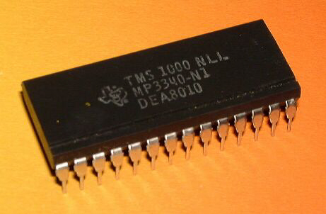
A microprocessor is a computer processor (computing), processor for which the data processing logic and control is included on a single integrated circuit (IC), or a small number of ICs. The microprocessor contains the arithmetic, logic, and control circuitry required to perform the functions of a computer's central processing unit (CPU). The IC is capable of interpreting and executing program instructions and performing arithmetic operations. The microprocessor is a multipurpose, Clock signal, clock-driven, Processor register, register-based, digital integrated circuit that accepts binary code, binary data as input, processes it according to instruction (computing), instructions stored in its computer memory, memory, and provides results (also in binary form) as output. Microprocessors contain both combinational logic and sequential logic, sequential digital logic, and operate on numbers and symbols represented in the binary number system. The integration of a whole CPU on ... [...More Info...] [...Related Items...] OR: [Wikipedia] [Google] [Baidu] |
Printed Circuit Board Milling
Printed circuit board milling (also: isolation milling) is the milling process used for removing areas of copper from a sheet of printed circuit board (PCB) material to recreate the pads, signal traces and structures according to patterns from a digital circuit board plan known as a ''layout file''. Similar to the more common and well known chemical PCB etch process, the PCB milling process is subtractive: material is removed to create the electrical isolation and ground planes required. However, unlike the chemical etch process, PCB milling is typically a non-chemical process and as such it can be completed in a typical office or lab environment without exposure to hazardous chemicals. High quality circuit boards can be produced using either process. In the case of PCB milling, the quality of a circuit board is chiefly determined by the system's true, or weighted, milling accuracy and control as well as the condition (sharpness, temper) of the milling bits and their respective f ... [...More Info...] [...Related Items...] OR: [Wikipedia] [Google] [Baidu] |
Milling (machining)
Milling is the process of machining using rotary Milling cutter, cutters to remove material by advancing a cutter into a workpiece. This may be done by varying directions on one or several axes, cutter head speed, and pressure. Milling covers a wide variety of different operations and machines, on scales from small individual parts to large, heavy-duty gang milling operations. It is one of the most commonly used processes for machining custom parts to precise tolerances. Milling can be done with a wide range of machine tools. The original class of machine tools for milling was the milling machine (often called a mill). After the advent of computer numerical control (CNC) in the 1960s, milling machines evolved into ''machining centers'': milling machines augmented by automatic tool changers, tool magazines or carousels, CNC capability, coolant systems, and enclosures. Milling centers are generally classified as vertical machining centers (VMCs) or horizontal machining centers (HMCs ... [...More Info...] [...Related Items...] OR: [Wikipedia] [Google] [Baidu] |
3D Printer
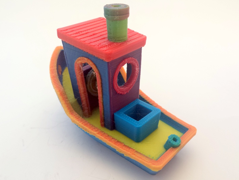
3D printing, or additive manufacturing, is the construction of a three-dimensional object from a CAD model or a digital 3D model. It can be done in a variety of processes in which material is deposited, joined or solidified under computer control, with the material being added together (such as plastics, liquids or powder grains being fused), typically layer by layer. In the 1980s, 3D printing techniques were considered suitable only for the production of functional or aesthetic prototypes, and a more appropriate term for it at the time was rapid prototyping. , the precision, repeatability, and material range of 3D printing have increased to the point that some 3D printing processes are considered viable as an industrial-production technology; in this context, the term ''additive manufacturing'' can be used synonymously with ''3D printing''. One of the key advantages of 3D printing is the ability to produce very complex shapes or geometries that would be otherwise infeasibl ... [...More Info...] [...Related Items...] OR: [Wikipedia] [Google] [Baidu] |
Rapid Prototyping
Rapid prototyping is a group of techniques used to quickly fabricate a scale model of a physical part or assembly using three-dimensional computer aided design ( CAD) data. Construction of the part or assembly is usually done using 3D printing technology. The first methods for rapid prototyping became available in mid 1987 and were used to produce models and prototype parts. Today, they are used for a wide range of applications and are used to manufacture production-quality parts in relatively small numbers if desired without the typical unfavorable short-run economics. This economy has encouraged online service bureaus. Historical surveys of RP technology start with discussions of simulacra production techniques used by 19th-century sculptors. Some modern sculptors use the progeny technology to produce exhibitions and various objects. The ability to reproduce designs from a dataset has given rise to issues of rights, as it is now possible to interpolate volumetric data from 2 ... [...More Info...] [...Related Items...] OR: [Wikipedia] [Google] [Baidu] |
IIT Kanpur
The Indian Institute of Technology Kanpur (IIT- Kanpur or IIT-K) is a public institute of technology located in Kanpur, Uttar Pradesh, India. As an Indian Institute of Technology (IIT), it was declared an Institute of National Importance by the Government of India under the Institutes of Technology Act. IIT Kanpur has been occasionally ranked among the best academic institutions in India. As of January 2025, at least 17 Padma Shri, 4 Padma Bhushan, 1 Padma Vibhushan, and 33 Shanti Swarup Bhatnagar Prize recipients have been affiliated with IIT Kanpur as alumni or faculty members. History IIT Kanpur was established by an Act of Parliament in 1960 by the Government of India. The institute was started in December 1959 in a room in the canteen building of the Harcourt Butler Technological University at Agricultural Gardens in Kanpur. In 1963, the institute moved to its present location, on the Grand Trunk Road near Kalyanpur locality in Kanpur district. The campus, which is p ... [...More Info...] [...Related Items...] OR: [Wikipedia] [Google] [Baidu] |


