|
Electron Channelling Contrast Imaging
Electron channelling contrast imaging (ECCI) is a scanning electron microscope (SEM) diffraction technique used in the study of defects in materials. These can be dislocations or stacking faults that are close to the surface of the sample, low angle grain boundaries or atomic steps. Unlike the use of transmission electron microscopy (TEM) for the investigation of dislocations, the ECCI approach has been called a rapid and non-destructive characterisation technique Mechanism The word channelling in ECCI, and, similarly, in electron channelling patterns refers to diffraction of the electron beam on its way in the sample. With enough spatial resolution, very small crystal imperfections would change the phase of the incident electron wave-function, and this, in turn, would be reflected in the backscattering probability, showing up as ''contrast'' (sharp change in backscattered intensity) close to a dislocation Background While we now talk about ECCI being a SEM technique, there w ... [...More Info...] [...Related Items...] OR: [Wikipedia] [Google] [Baidu] |
Scanning Electron Microscope
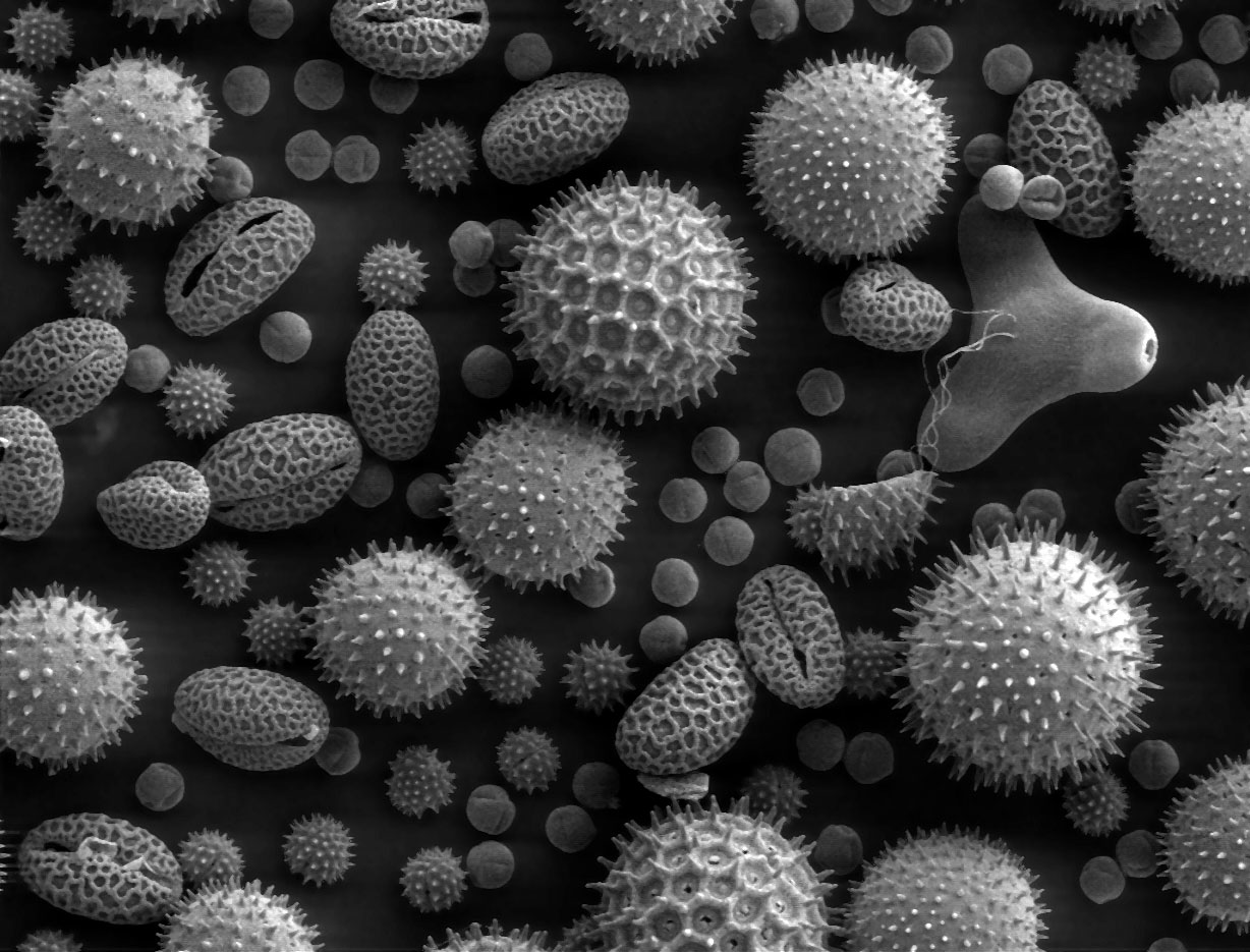
A scanning electron microscope (SEM) is a type of electron microscope that produces images of a sample by scanning the surface with a focused beam of electrons. The electrons interact with atoms in the sample, producing various signals that contain information about the surface topography and composition. The electron beam is scanned in a raster scan pattern, and the position of the beam is combined with the intensity of the detected signal to produce an image. In the most common SEM mode, secondary electrons emitted by atoms excited by the electron beam are detected using a secondary electron detector ( Everhart–Thornley detector). The number of secondary electrons that can be detected, and thus the signal intensity, depends, among other things, on specimen topography. Some SEMs can achieve resolutions better than 1 nanometer. Specimens are observed in high vacuum in a conventional SEM, or in low vacuum or wet conditions in a variable pressure or environmental SEM, an ... [...More Info...] [...Related Items...] OR: [Wikipedia] [Google] [Baidu] |
Diffraction
Diffraction is the deviation of waves from straight-line propagation without any change in their energy due to an obstacle or through an aperture. The diffracting object or aperture effectively becomes a secondary source of the Wave propagation, propagating wave. Diffraction is the same physical effect as Wave interference, interference, but interference is typically applied to superposition of a few waves and the term diffraction is used when many waves are superposed. Italian scientist Francesco Maria Grimaldi coined the word ''diffraction'' and was the first to record accurate observations of the phenomenon in 1660 in science, 1660. In classical physics, the diffraction phenomenon is described by the Huygens–Fresnel principle that treats each point in a propagating wavefront as a collection of individual spherical wavelets. The characteristic pattern is most pronounced when a wave from a Coherence (physics), coherent source (such as a laser) encounters a slit/aperture tha ... [...More Info...] [...Related Items...] OR: [Wikipedia] [Google] [Baidu] |
Dislocation
In materials science, a dislocation or Taylor's dislocation is a linear crystallographic defect or irregularity within a crystal structure that contains an abrupt change in the arrangement of atoms. The movement of dislocations allow atoms to slide over each other at low stress levels and is known as ''glide'' or Slip (materials science), slip. The crystalline order is restored on either side of a ''glide dislocation'' but the atoms on one side have moved by one position. The crystalline order is not fully restored with a ''partial dislocation''. A dislocation defines the boundary between ''slipped'' and ''unslipped'' regions of material and as a result, must either form a complete loop, intersect other dislocations or defects, or extend to the edges of the crystal. A dislocation can be characterised by the distance and direction of movement it causes to atoms which is defined by the Burgers vector. Plasticity (physics), Plastic deformation of a material occurs by the creation and ... [...More Info...] [...Related Items...] OR: [Wikipedia] [Google] [Baidu] |
Stacking Fault
In crystallography, a stacking fault is a planar defect that can occur in crystalline materials.Fine, Morris E. (1921). "Introduction to Chemical and Structural Defects in Crystalline Solids", in ''Treatise on Solid State Chemistry Volume 1'', Springer. Crystalline materials form repeating patterns of layers of atoms. Errors can occur in the sequence of these layers and are known as stacking faults. Stacking faults are in a higher energy state which is quantified by the formation enthalpy per unit area called the stacking-fault energy. Stacking faults can arise during crystal growth or from plastic deformation. In addition, dislocations in low stacking-fault energy materials typically dissociate into an ''extended dislocation'', which is a stacking fault bounded by partial dislocations. The most common example of stacking faults is found in close-packed crystal structures. Face-centered cubic (fcc) structures differ from hexagonal close packed (hcp) structures only in stacking ... [...More Info...] [...Related Items...] OR: [Wikipedia] [Google] [Baidu] |
Grain Boundary
In materials science, a grain boundary is the interface between two grains, or crystallites, in a polycrystalline material. Grain boundaries are two-dimensional defects in the crystal structure, and tend to decrease the electrical and thermal conductivity of the material. Most grain boundaries are preferred sites for the onset of corrosion and for the precipitation of new phases from the solid. They are also important to many of the mechanisms of creep. On the other hand, grain boundaries disrupt the motion of dislocations through a material, so reducing crystallite size is a common way to improve mechanical strength, as described by the Hall–Petch relationship. High and low angle boundaries It is convenient to categorize grain boundaries according to the extent of misorientation between the two grains. ''Low-angle grain boundaries'' (''LAGB'') or ''subgrain boundaries'' are those with a misorientation less than about 15 degrees. Generally speaking they are composed of ... [...More Info...] [...Related Items...] OR: [Wikipedia] [Google] [Baidu] |
Transmission Electron Microscopy
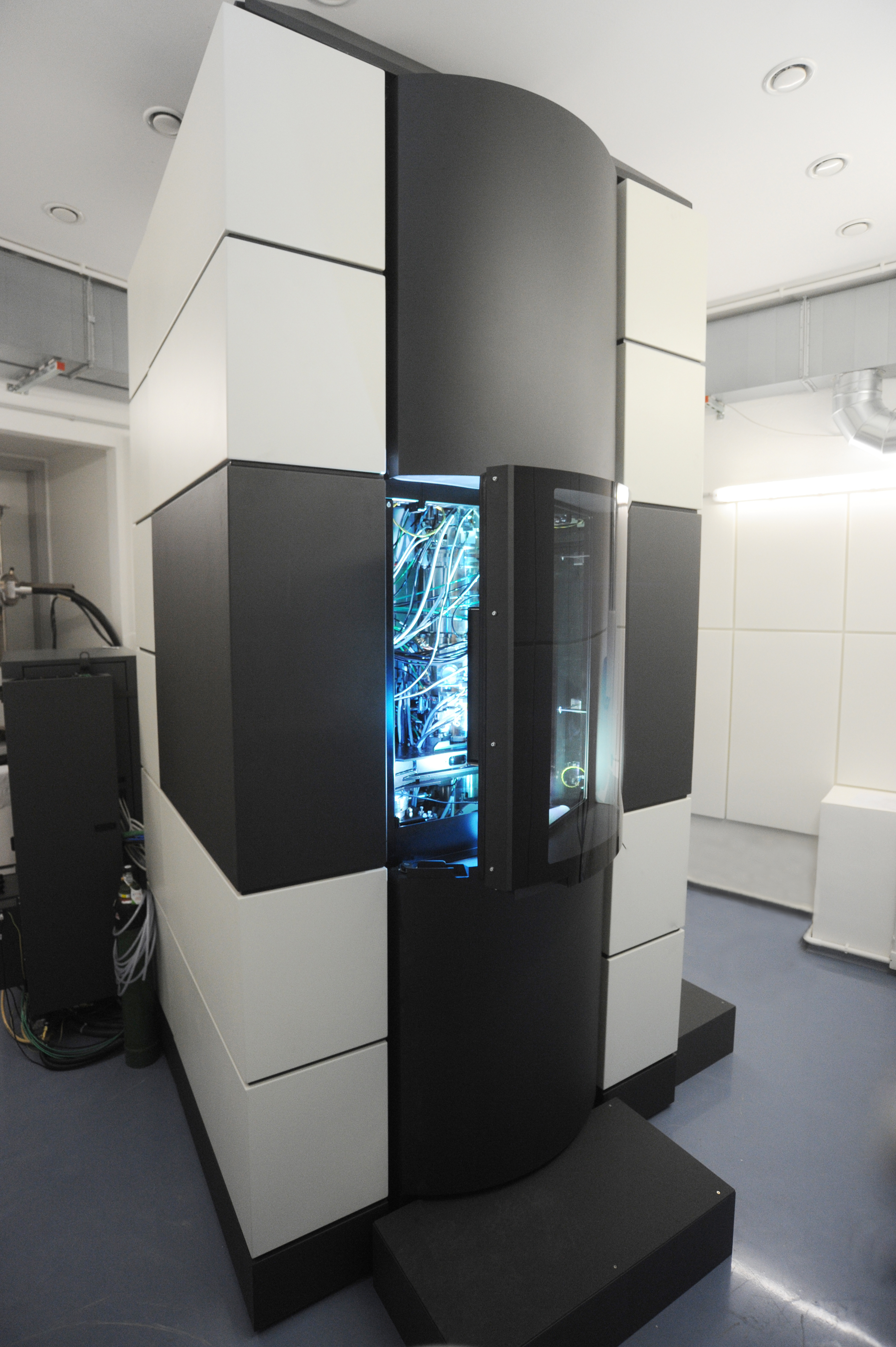
Transmission electron microscopy (TEM) is a microscopy technique in which a beam of electrons is transmitted through a specimen to form an image. The specimen is most often an ultrathin section less than 100 nm thick or a suspension on a grid. An image is formed from the interaction of the electrons with the sample as the beam is transmitted through the specimen. The image is then magnified and focused onto an imaging device, such as a fluorescent screen, a layer of photographic film, or a detector such as a scintillator attached to a charge-coupled device or a direct electron detector. Transmission electron microscopes are capable of imaging at a significantly higher resolution than light microscopes, owing to the smaller de Broglie wavelength of electrons. This enables the instrument to capture fine detail—even as small as a single column of atoms, which is thousands of times smaller than a resolvable object seen in a light microscope. Transmission electron micr ... [...More Info...] [...Related Items...] OR: [Wikipedia] [Google] [Baidu] |
Field Emission Gun
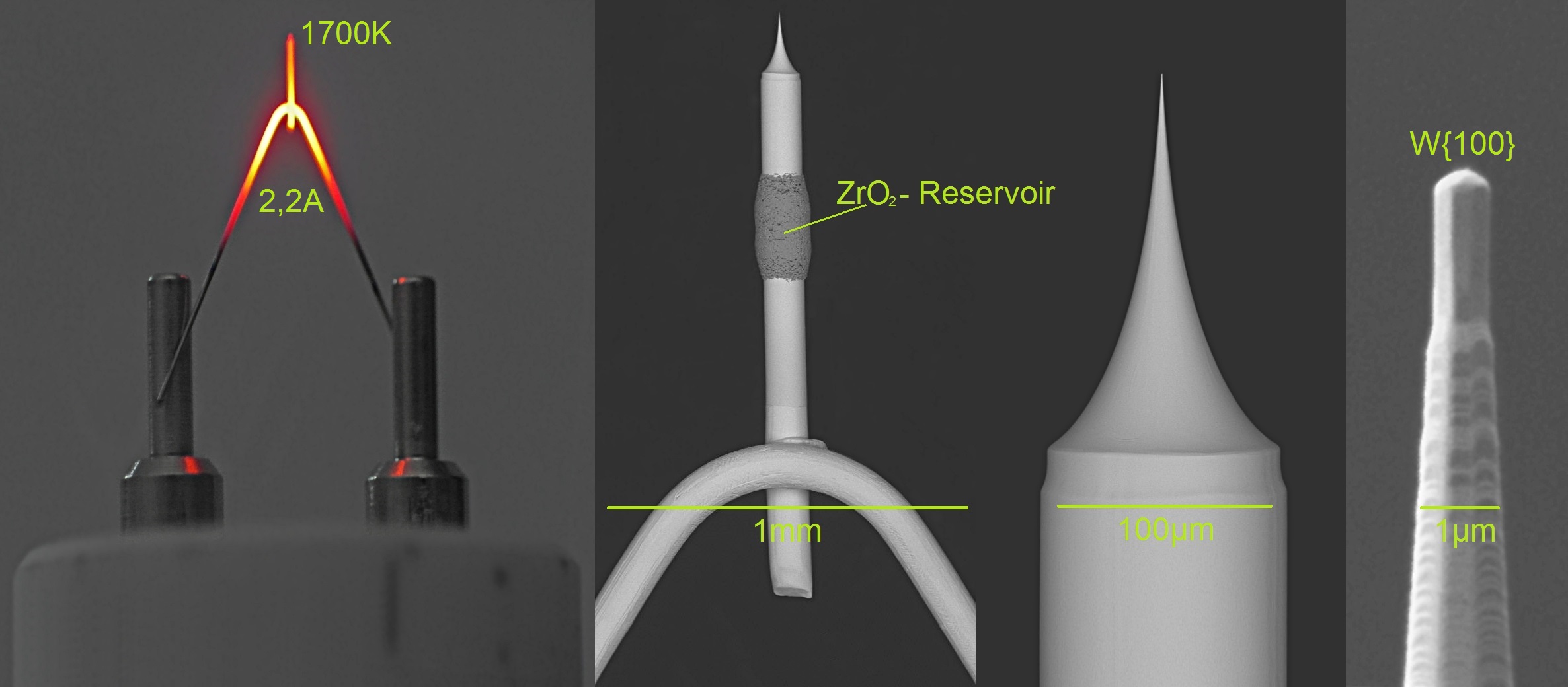
A field emission gun (FEG) is a type of electron gun in which a sharply pointed Müller-type emitter is held at several kilovolts negative potential relative to a nearby electrode, so that there is sufficient potential gradient at the emitter surface to cause field electron emission. Emitters are either of cold-cathode type, usually made of single crystal tungsten sharpened to a tip radius of about 100 nm, or of the Walter H. Schottky, Schottky type, in which thermionic emission is enhanced by barrier lowering in the presence of a high electric field. Schottky emitters are made by coating a tungsten tip with a layer of zirconium oxide (ZrO2) decreasing the work function of the tip by approximately 2.7 electronvolt, eV. In electron microscopes, a field emission gun is used to produce an electron beam that is smaller in diameter, more Coherence (physics), coherent and with up to three orders of magnitude greater current density or brightness than can be achieved with conventio ... [...More Info...] [...Related Items...] OR: [Wikipedia] [Google] [Baidu] |
Angus Wilkinson
Angus J. Wilkinson is a professor of materials science based at the Department of Materials, University of Oxford. He is a specialist in micromechanics of materials and electron microscopy. Biography Wilkinson is from Spexhall, Suffolk. He obtained a bachelor's degree in chemical physics and PhD in engineering from the University of Bristol. He moved to Department of Materials, University of Oxford as postdoctoral researcher in early 1990s. Wilkinson research focuses on materials science, particularly in the areas of electron backscatter diffraction (EBSD), deformation mechanisms, and microstructural characterisation of materials. His research explores plasticity, strain localisation, and the mechanical behaviour of materials at the microscale, often using advanced microscopy techniques to study stress and deformation in metals and alloys. Wilkinson developed the HR-EBSD method for mapping strain and dislocation density at high spatial resolution at the micron scale. Wi ... [...More Info...] [...Related Items...] OR: [Wikipedia] [Google] [Baidu] |
Electron Backscatter Diffraction
Electron backscatter diffraction (EBSD) is a scanning electron microscopy (SEM) technique used to study the Crystallography, crystallographic structure of materials. EBSD is carried out in a scanning electron microscope equipped with an EBSD detector comprising at least a Phosphorescence, phosphorescent screen, a compact lens and a low-light Charge-coupled device, camera. In the microscope an incident beam of electrons hits a tilted sample. As backscattered electrons leave the sample, they interact with the atoms and are both elastically Electron diffraction, diffracted and lose energy, leaving the sample at various scattering angles before reaching the phosphor screen forming Kikuchi lines (physics), Kikuchi patterns (EBSPs). The EBSD spatial resolution depends on many factors, including the nature of the material under study and the sample preparation. They can be indexed to provide information about the material's grain Crystal structure, structure, grain Electron crystallogr ... [...More Info...] [...Related Items...] OR: [Wikipedia] [Google] [Baidu] |
Carol Trager-Cowan
Carol Trager-Cowan is a Scottish physicist who is a Reader (Associate Professor) in physics and Science Communicator at the University of Strathclyde. She works on scanning electron microscopy, including Electron backscatter diffraction (EBSD), diffraction contrast and cathodoluminescence imaging.Carol Trager-Cowan's Education and early career Trager-Cowan was an undergraduate student at the University of Glasgow, where she earned a bachelor's degree in natural philosophy in 1983. She moved to the University of St Andrews for her graduate studies, earning a master's degree in 1984. Her dissertation considered hot electrons in Gallium arsenide. She moved to Royal Holloway, University of London for her doctorate, completing her thesis on electrostatic electron lenses in 1987 supervised by . She completed experimental and theoretical investigations into electrostatic lenses. Research and career Trager-Cowan is a Reader (Associate Professor) in Physics at the University of S ... [...More Info...] [...Related Items...] OR: [Wikipedia] [Google] [Baidu] |
Electron Microscopy
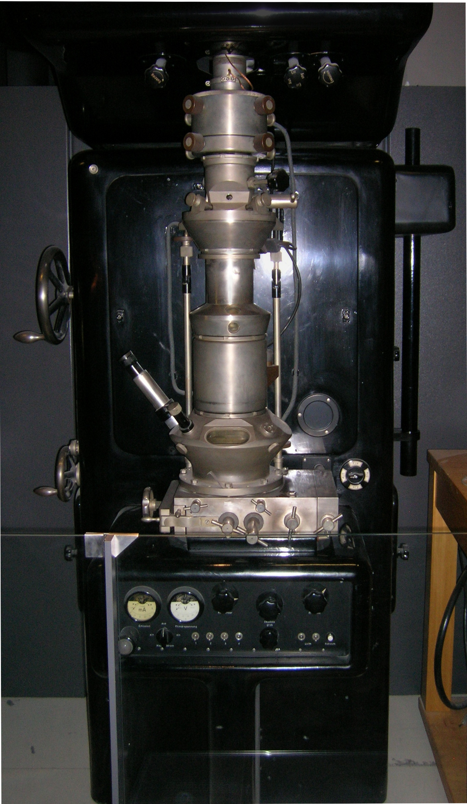
An electron microscope is a microscope that uses a beam of electrons as a source of illumination. It uses electron optics that are analogous to the glass lenses of an optical light microscope to control the electron beam, for instance focusing it to produce magnified images or electron diffraction patterns. As the wavelength of an electron can be up to 100,000 times smaller than that of visible light, electron microscopes have a much higher resolution of about 0.1 nm, which compares to about 200 nm for light microscopes. ''Electron microscope'' may refer to: * Transmission electron microscope (TEM) where swift electrons go through a thin sample * Scanning transmission electron microscope (STEM) which is similar to TEM with a scanned electron probe * Scanning electron microscope (SEM) which is similar to STEM, but with thick samples * Electron microprobe similar to a SEM, but more for chemical analysis * Low-energy electron microscope (LEEM), used to image surfaces * ... [...More Info...] [...Related Items...] OR: [Wikipedia] [Google] [Baidu] |


