Nanolaser on:
[Wikipedia]
[Google]
[Amazon]
A nanolaser is a
 Since roughly 2010, there has been progress in nanolaser technology, and new types of nanolasers have been developed, such as parity-time symmetry laser, bound states in the continuum laser and
 Compared with conventional lasers, nanolasers show distinct properties and capabilities. The biggest advantages of nanolasers are their ultra-small physical volumes to improve energy efficiencies, decrease lasing thresholds, and achieve high modulation speeds.
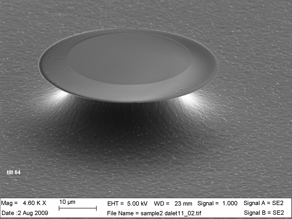 A microdisk laser is a very small laser consisting of a disk with
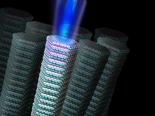 Semiconductor nanowire lasers have a quasi-one-dimensional structure with diameters ranging from a few nanometers to a few hundred nanometers and lengths ranging from hundreds of nanometers to a few microns. The width of nanowires is large enough to ignore the quantum size effect, but they are high quality one-dimensional
 Nanolaser based on surface plasmon is known as plasmonic nanolaser, whose size far exceeds the diffraction limit of light. Especially, if a plasmonic nanolaser is nanoscopic in three dimensions, it is also called as
  SPPs are electromagnetic waves that propagate along the interface between metal and medium, and their intensities decay gradually in the direction perpendicular to the propagation interface. In 2008, Oulton experimentally validated a plasma nanowire laser consisting of a thin dielectric layer with a low reflectivity growing on a metal surface and a gain layer with a high
 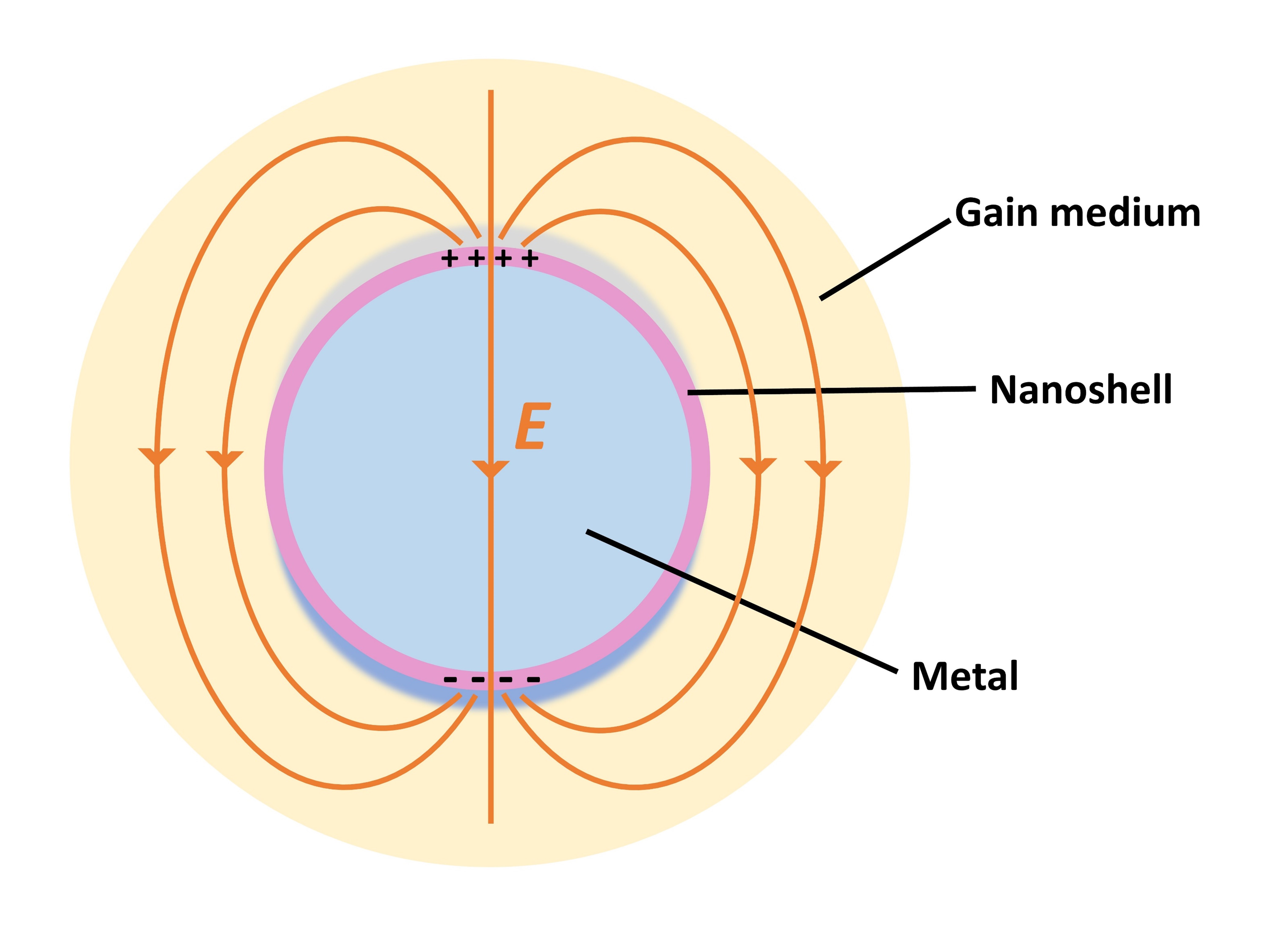 The LSP mode exists in a variety of different metal nanostructures, such as metal
"Spaser": The future of nanolaser technologyBreakthrough in the Creation of Electrically Driven Nanolasers for Integrated Circuits
Quantum optics Photonics American inventions Laser types
laser
A laser is a device that emits light through a process of optical amplification based on the stimulated emission of electromagnetic radiation. The word "laser" is an acronym for "light amplification by stimulated emission of radiation". The fi ...
that has nanoscale
The nanoscopic scale (or nanoscale) usually refers to structures with a length scale applicable to nanotechnology, usually cited as 1–100 nanometers (nm). A nanometer is a billionth of a meter. The nanoscopic scale is (roughly speaking) a lo ...
dimensions and it refers to a micro-/nano- device which can emit light with light or electric excitation of nanowires or other nanomaterials that serve as resonator
A resonator is a device or system that exhibits resonance or resonant behavior. That is, it naturally oscillates with greater amplitude at some frequencies, called resonant frequencies, than at other frequencies. The oscillations in a resonator ...
s. A standard feature of nanolasers includes their light confinement on a scale approaching or suppressing the diffraction limit of light. These tiny lasers can be modulated quickly and, combined with their small footprint
Footprints are the impressions or images left behind by a person walking or running. Hoofprints and pawprints are those left by animals with hooves or paws rather than feet, while "shoeprints" is the specific term for prints made by shoes. The ...
, this makes them ideal candidates for on-chip optical computing.
History
Albert Einstein
Albert Einstein ( ; ; 14 March 1879 – 18 April 1955) was a German-born theoretical physicist, widely acknowledged to be one of the greatest and most influential physicists of all time. Einstein is best known for developing the theory ...
proposed the stimulated emission in 1916, which contributed to the first demonstration of laser in 1961. From then on, people have been pursuing the miniaturization of lasers for more compact size and less energy consumption all the time. Since people noticed that light has different interactions with matter at the nanoscale in the 1990s, significant progress has been made to achieve the miniaturization of lasers and increase power conversion efficiency. Various types of nanolasers have been developed over the past decades.
In the 1990s, some intriguing designs of microdisk laser and photonic crystal
A photonic crystal is an optical nanostructure in which the refractive index changes periodically. This affects the propagation of light in the same way that the structure of natural crystals gives rise to X-ray diffraction and that the atomic ...
laser were demonstrated to have cavity size or energy volume with micro-/nano- diameters and approach the diffraction limit of light. Photoluminescence behavior of bulk ZnO nanowires was first reported in 2001 by Prof. Peidong Yang from the University of California, Berkeley
The University of California, Berkeley (UC Berkeley, Berkeley, Cal, or California) is a public land-grant research university in Berkeley, California. Established in 1868 as the University of California, it is the state's first land-grant u ...
and it opened the door to the study of nanowire nanolasers. These designs still do not exceed the diffraction limit until the demonstration of plasmonic lasers or spasers.
David J. Bergman and Mark Stockman first proposed amplified surface plasmon
Surface plasmons (SPs) are coherent delocalized electron oscillations that exist at the interface between any two materials where the real part of the dielectric function changes sign across the interface (e.g. a metal-dielectric interface, such ...
waves by stimulated emission and coined the term spaser
A spaser or plasmonic laser is a type of laser which aims to confine light at a subwavelength scale far below Rayleigh's diffraction limit of light, by storing some of the light energy in electron oscillations called surface plasmon polaritons. ...
as "surface plasmon amplification by stimulated emission of radiation" in 2003. Until 2009, the plasmonic nanolasers or spasers were first achieved experimentally, which were regarded as the smallest nanolasers at that time.
 Since roughly 2010, there has been progress in nanolaser technology, and new types of nanolasers have been developed, such as parity-time symmetry laser, bound states in the continuum laser and
 photonic topological insulator Photonic topological insulators are artificial electromagnetic materials that support topologically non-trivial, unidirectional states of light. Photonic topological phases are classical electromagnetic wave analogues of electronic topological phase ...
s laser.
Comparison with conventional lasers
While sharing many similarities with standard lasers, nanolasers maintain many unique features and differences from the conventional lasers due to the fact that light interacts differently with matter at the nanoscale.Mechanism
Similar to the conventional lasers, nanolasers also based on stimulated emission which was proposed by Einstein; the main difference between nanolaser and the conventional ones in mechanism is light confinement. The resonator or cavity plays an important role in selecting the light with a certain frequency and the same direction as the most priority amplification and suppressing the other light to achieve the confinement of light. For conventional lasers, Fabry–Pérot cavity with two parallel reflection mirrors is applied. In this case, light could be confined to a maximum of half its wavelength and such limit is deemed the diffraction limit of light. To approach or decrease the diffraction limit of light, one way is to improve thereflectivity
The reflectance of the surface of a material is its effectiveness in Reflection (physics), reflecting radiant energy. It is the fraction of incident electromagnetic power that is reflected at the boundary. Reflectance is a component of the respon ...
of gain medium
The active laser medium (also called gain medium or lasing medium) is the source of optical gain within a laser. The gain results from the stimulated emission of photons through electronic or molecular transitions to a lower energy state from a h ...
, such as using photonic bandgap and nanowires. Another effective way to exceed the diffraction limit is to convert light into surface plasmons in nanostructuralized metals, for amplification in cavity. Recently, new mechanisms of strong light confinement for nanolasers including parity–time symmetry, photonic topological insulators, and bound states in the continuum have been proposed.
Properties
 Compared with conventional lasers, nanolasers show distinct properties and capabilities. The biggest advantages of nanolasers are their ultra-small physical volumes to improve energy efficiencies, decrease lasing thresholds, and achieve high modulation speeds.
Types of nanolasers
Microdisk laser
quantum well
A quantum well is a potential well with only discrete energy values.
The classic model used to demonstrate a quantum well is to confine particles, which were initially free to move in three dimensions, to two dimensions, by forcing them to occupy ...
structures built into it. Its dimensions can exist on the micro-scale or nano-scale. Microdisk lasers use a whispering-gallery mode resonant cavity. The light in cavity travels around the perimeter of the disk and the total internal reflection of photons can result in a strong light confinement and a high quality factor, which means a powerful ability of the microcavity to store the energy of photons coupled into the cavity.
Photonic crystal laser
Photonic crystal
A photonic crystal is an optical nanostructure in which the refractive index changes periodically. This affects the propagation of light in the same way that the structure of natural crystals gives rise to X-ray diffraction and that the atomic ...
lasers utilize periodic dielectric
In electromagnetism, a dielectric (or dielectric medium) is an electrical insulator that can be polarised by an applied electric field. When a dielectric material is placed in an electric field, electric charges do not flow through the mate ...
structures with different refractive indices; light can be confined with the use of a photonic crystal microcavity. In dielectric materials, there is orderly spatial distribution. When there is a defect in the periodic structure, the two-dimensional or three-dimensional photonic crystal structure will confine the light in the space of the diffractive limit and produce the Fano resonance phenomenon, which means a high quality factor with a strong light confinement for lasers. The fundamental feature of photonic crystals is the photonic bandgap, that is, the light whose frequency falls in the photonic band gap cannot propagate in the crystal structure, thus resulting in a high reflectivity for incident light and a strong confinement of light to a small volume of wavelength scale. The appearance of photonic crystals makes the spontaneous emission in the photon gap completely suppressed. But the high cost of photonic crystal impedes the development and spreading applications of photonic crystal lasers.
Nanowire nanolaser
 Semiconductor nanowire lasers have a quasi-one-dimensional structure with diameters ranging from a few nanometers to a few hundred nanometers and lengths ranging from hundreds of nanometers to a few microns. The width of nanowires is large enough to ignore the quantum size effect, but they are high quality one-dimensional
 waveguide
A waveguide is a structure that guides waves, such as electromagnetic waves or sound, with minimal loss of energy by restricting the transmission of energy to one direction. Without the physical constraint of a waveguide, wave intensities de ...
s with cylindrical, rectangular, trigonal, and hexagonal cross-sections. The quasi-one-dimensional structure and high reflectivity of nanowire laser makes it have good optical waveguide and the ability of light confinement. Nanowire lasers are similar to Fabry–Pérot cavity in mechanism. High reflectivity of nanowire and flat end facets of the wire constitute a good resonant cavity, in which photons can be bound between the two ends of the nanowire to limit the light energy to the axial direction of the nanowire, thus meeting the conditions for laser formation. Polygonal nanowires can form a nearly circular cavity in cross section that supports whispering-gallery mode.
Plasmonic nanolaser
 Nanolaser based on surface plasmon is known as plasmonic nanolaser, whose size far exceeds the diffraction limit of light. Especially, if a plasmonic nanolaser is nanoscopic in three dimensions, it is also called as
 spaser
A spaser or plasmonic laser is a type of laser which aims to confine light at a subwavelength scale far below Rayleigh's diffraction limit of light, by storing some of the light energy in electron oscillations called surface plasmon polaritons. ...
, which is known to have the smallest cavity size and mode size. Design of plasmonic nanolaser has become one of the most effective technology methods for laser miniaturization at present. A little bit different from the conventional lasers, a typical configuration of plasmonic nanolaser includes a process of energy transfer
In physics, energy (from Ancient Greek: ἐνέργεια, ''enérgeia'', “activity”) is the quantitative property that is transferred to a body or to a physical system, recognizable in the performance of work and in the form of heat ...
to convert photons into surface plasmons. In plasmonic nanolaser or spaser, the exciton is not photons anymore but surface plasmon polariton. Surface plasmons are collective oscillations of free electrons on metal surfaces under the action of external electromagnetic fields. According to their manifestations, the cavity mode in plasmonic nanolasers can be divided into the propagating surface plasmon polaritons (SPPs) and the non-propagating localized surface plasmons (LSPs).
 SPPs are electromagnetic waves that propagate along the interface between metal and medium, and their intensities decay gradually in the direction perpendicular to the propagation interface. In 2008, Oulton experimentally validated a plasma nanowire laser consisting of a thin dielectric layer with a low reflectivity growing on a metal surface and a gain layer with a high
 refractive index
In optics, the refractive index (or refraction index) of an optical medium is a dimensionless number that gives the indication of the light bending ability of that medium.
The refractive index determines how much the path of light is bent, or ...
semiconductor nanowire. In this structure, the electromagnetic field can be transferred from the metal layer to the intermediate gap layer, so that the mode energy is highly concentrated, thus greatly reducing the energy loss in the metal.
 The LSP mode exists in a variety of different metal nanostructures, such as metal
 nanoparticle
A nanoparticle or ultrafine particle is usually defined as a particle of matter that is between 1 and 100 nanometres (nm) in diameter. The term is sometimes used for larger particles, up to 500 nm, or fibers and tubes that are less than 10 ...
s (nanospheres, nanorods, nanocubes, etc.) and arrays of nanoparticles. Unlike the propagating surface plasmon polaritons, the localized surface plasmon does not propagate along the surface, but oscillates back and forth in the nanostructure in the form of standing waves. When light is incident to the surface of a metal nanoparticles, it causes a real displacement of the surface charge relative to the ions. The attraction between electrons and ions allows for the oscillation of electrode cloud and the formation of local surface from polarization excimer. The oscillation of electrons is determined by the geometrical boundaries of different metal nanoparticles. When its resonance frequency is consistent with the incident electromagnetic field, it will form the localized surface plasmon resonance. In 2009, Mikhail A. Noginov of Norfolk State University
Norfolk State University (NSU) is a public historically black university in Norfolk, Virginia. It is a member of the Thurgood Marshall College Fund and Virginia High-Tech Partnership.
History
The institution was founded on September 18, 1935 ...
in the United States
The United States of America (U.S.A. or USA), commonly known as the United States (U.S. or US) or America, is a country primarily located in North America. It consists of 50 states, a federal district, five major unincorporated territori ...
successfully verified the LSPs-based nanolaser for the first time. The nanolaser in this paper was composed of an Au core providing the plasmon mode and a silicon dioxide doped with OG-488 dye providing the gain medium. The diameter of the Au core was 14 nm, the thickness of the silica layer was 15 nm, and the diameter of the whole device was only 44 nm, which was the smallest nanolaser at that time.
New types of nanolasers
In addition, there have been some new types of nanolasers developed in recent years to approach the diffraction limit. Parity-time symmetry is related to a balance of optical gain and loss in a coupled cavity system. When the gain–loss contrast and coupling constant between two identical, closely located cavities are controlled, the phase transition of lasing modes occurs at an exceptional point. Bound states in the continuum laser confines light in an open system via the elimination of radiation states through destructive interference between resonant modes. A photonic topological insulator laser is based on topological insulators optical mode, where the topological states is confined within the cavity boundaries and they can be used for the formation of laser. All of those new types of nanolasers have high quality factor and can achieve cavity size and mode size approaching the diffraction limit of the light.Applications
Due to the unique capabilities including low lasing thresholds, high energy efficiencies and high modulation speeds, nanolasers show great potentials for practical applications in the fields of materials characterization, integrated optical interconnects, and sensing.Nanolasers for material characterization
The intense optical fields of such a laser also enable the enhancement effect innon-linear optics
Nonlinear optics (NLO) is the branch of optics that describes the behaviour of light in ''nonlinear media'', that is, media in which the polarization density P responds non-linearly to the electric field E of the light. The non-linearity is typica ...
or surface-enhanced-raman-scattering ( SERS). Nanowire nanolasers can be capable of optical detection at the scale of a single molecule with high resolution and ultrafast modulation.
Nanolasers for integrated optical interconnects
Internet is developing at an extremely high speed with large energy consumption fordata communication
Data transmission and data reception or, more broadly, data communication or digital communications is the transfer and reception of data in the form of a digital bitstream or a digitized analog signal transmitted over a point-to-point or ...
. The high energy efficiency of nanolasers plays an important role in decreasing energy consumption for future society.
Nanolasers for sensing
Plasmonic nanolaser sensors have recently been demonstrated that can detect specific molecules in air and be used for opticalbiosensor
A biosensor is an analytical device, used for the detection of a chemical substance, that combines a biological component with a physicochemical detector.
The ''sensitive biological element'', e.g. tissue, microorganisms, organelles, cell rece ...
s. Molecules can modify the surface of metal nanoparticles and impact the surface recombination velocity of gain medium of a plasmonic nanolaser, which contributes to the sensing mechanism of plasmonic nanolasers.
Challenges
Although nanolasers have shown great potential, there are still some challenges towards the large-scale use of nanolasers, for example, electrically injected nanolasers, cavity configuration engineering and metal quality improvement. For nanolasers, the realization of electrically injected or pumped operation at room temperature is a key step towards its practical application. However, most nanolaser are optically pumped and the realization of electrically injected nanolasers is still a main technical challenge at present. Only a few studies have reported electrically injected nanolasers. Moreover, it still remains a challenge to realize cavity configuration engineering and metal quality improvement, which are crucial to satisfy the high-performance requirement of nanolasers and achieve their applications. Recently, nanolaser arrays show great potential to increase the power efficiency and accelerate modulation speed.See also
* List of laser articles *Laser
A laser is a device that emits light through a process of optical amplification based on the stimulated emission of electromagnetic radiation. The word "laser" is an acronym for "light amplification by stimulated emission of radiation". The fi ...
*Spaser
A spaser or plasmonic laser is a type of laser which aims to confine light at a subwavelength scale far below Rayleigh's diffraction limit of light, by storing some of the light energy in electron oscillations called surface plasmon polaritons. ...
* Nanowire laser
References
{{ReflistExternal links
"Spaser": The future of nanolaser technology
Quantum optics Photonics American inventions Laser types