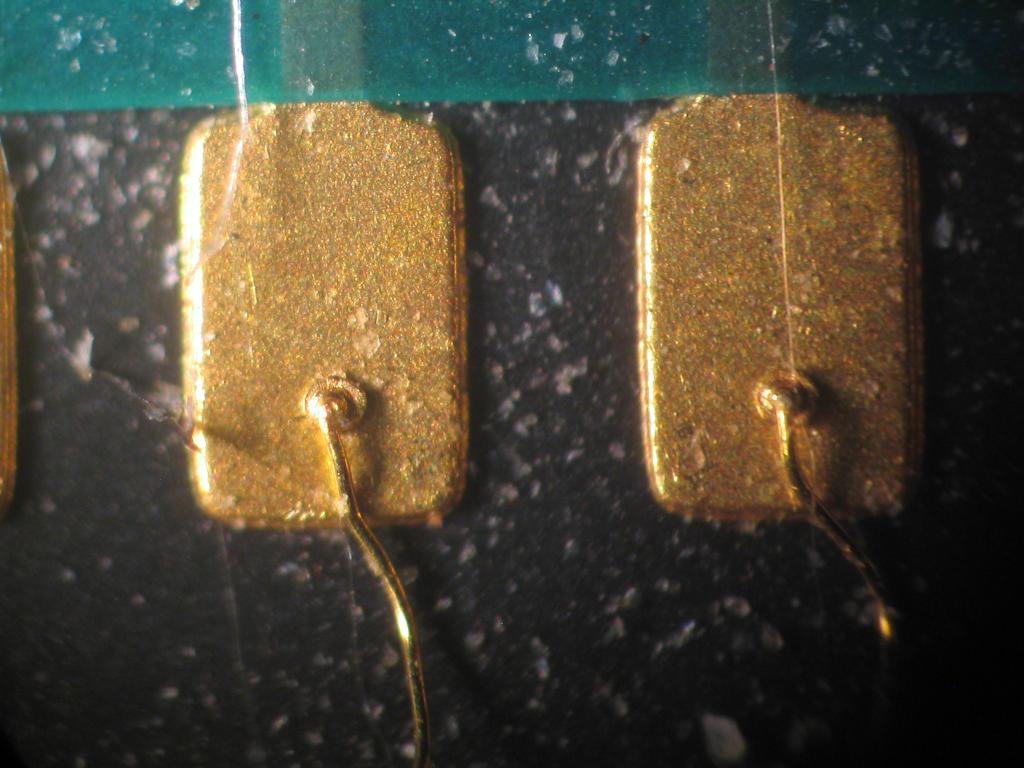
Contact pad on:
[Wikipedia]
[Google]
[Amazon]
 Contact pads or bond pads are designated surface areas of a
 Contact pads or bond pads are designated surface areas of a
 printed circuit board
A printed circuit board (PCB; also printed wiring board or PWB) is a medium used in electrical and electronic engineering to connect electronic components to one another in a controlled manner. It takes the form of a laminated sandwich str ...
(PCB) or die
Die, as a verb, refers to death, the cessation of life.
Die may also refer to:
Games
* Die, singular of dice, small throwable objects used for producing random numbers
Manufacturing
* Die (integrated circuit), a rectangular piece of a semicondu ...
of an integrated circuit
An integrated circuit or monolithic integrated circuit (also referred to as an IC, a chip, or a microchip) is a set of electronic circuits on one small flat piece (or "chip") of semiconductor material, usually silicon. Large numbers of tiny ...
.
Possibilities to contact to pads include solder
Solder (; NA: ) is a fusible metal alloy used to create a permanent bond between metal workpieces. Solder is melted in order to wet the parts of the joint, where it adheres to and connects the pieces after cooling. Metals or alloys suitable ...
ing, wirebonding, flip chip
Flip chip, also known as controlled collapse chip connection or its abbreviation, C4, is a method for interconnecting dies such as semiconductor devices, IC chips, integrated passive devices and microelectromechanical systems (MEMS), to extern ...
mounting, or probe needles.
Further reading
*Kraig Mitzner, ''Complete PCB Design Using OrCAD Capture and PCB Editor'', Newnes, 2009 . *Jing Li, ''Evaluation and Improvement of the Robustness of a PCB Pad in a Lead-free Environment'', ProQuest, 2007 . *Deborah Lea, Fredirikus Jonck, Christopher Hunt, ''Solderability Measurements of PCB Pad Finishes and Geometries'', National Physical Laboratory, 2001 . Electronic engineering Printed circuit board manufacturing {{Electronics-stub