Cadmium arsenide on:
[Wikipedia]
[Google]
[Amazon]
Cadmium arsenide ( Cd3 As2) is an inorganic
 Cadmium arsenide can be prepared as amorphous semiconductive
National Pollutant Inventory – Cadmium and compounds
{{Arsenides Arsenides Cadmium compounds II-V compounds
semimetal
A semimetal is a material with a very small overlap between the bottom of the conduction band and the top of the valence band.
According to electronic band theory, solids can be classified as insulators, semiconductors, semimetals, or metals ...
in the II-V family. It exhibits the Nernst effect
In physics and chemistry, the Nernst effect (also termed first Nernst–Ettingshausen effect, after Walther Nernst and Albert von Ettingshausen) is a thermoelectric (or thermomagnetic) phenomenon observed when a sample allowing electrical conduct ...
.
Properties
Thermal
Cd3As2 dissociates between 220 and 280 °C according to the reaction :2 Cd3As2(s) → 6 Cd(g) + As4(g) Anenergy barrier
In chemistry and physics, activation energy is the minimum amount of energy that must be provided for compounds to result in a chemical reaction. The activation energy (''E''a) of a reaction is measured in joules per mole (J/mol), kilojoules pe ...
was found for the nonstoichiometric vaporization of arsenic due to the irregularity of the partial pressures with temperature. The range of the energy gap is from 0.5 to 0.6 eV. Cd3As2 melts at 716 °C and changes phase at 615 °C/
Phase transition
Pure cadmium arsenide undergoes several phase transitions at high temperatures, making phases labeled α (stable), α’, α” (metastable), and β. At 593° the polymorphic transition α → β occurs. :α-Cd3As2 ↔ α’-Cd3As2 occurs at ~500 K. :α’-Cd3As2 ↔ α’’-Cd3As2 occurs at ~742 K and is a regular first order phase transition with marked hysteresis loop. :α”-Cd3As2 ↔ β-Cd3As2 occurs at 868 K. Single crystal x-ray diffraction was used to determine the lattice parameters of Cd3As2 between 23 and 700 °C. Transition α → α′ occurs slowly and therefore is most likely an intermediate phase. Transition α′ → α″ occurs much faster than α → α′ and has very small thermal hysteresis. This transition results in a change in the fourfold axis of the tetragonal cell, causingcrystal twinning
Crystal twinning occurs when two or more adjacent crystals of the same mineral are oriented so that they share some of the same crystal lattice points in a symmetrical manner. The result is an intergrowth of two separate crystals that are tightly ...
. The width of the loop is independent of the rate of heating although it becomes narrower after several temperature cycles.
Electronic
The compound cadmium arsenide has a lower vapor pressure (0.8 atm) than both cadmium and arsenic separately. Cadmium arsenide does not decompose when it is vaporized and re-condensed. Carrier Concentration in Cd3As2 are usually (1–4)×1018 electrons/cm3. Despite having high carrier concentrations, the electron mobilities are also very high (up to 10,000 cm2/(V·s) at room temperature). In 2014 Cd3As2 was shown to be asemimetal
A semimetal is a material with a very small overlap between the bottom of the conduction band and the top of the valence band.
According to electronic band theory, solids can be classified as insulators, semiconductors, semimetals, or metals ...
material analogous to graphene
Graphene () is an allotrope of carbon consisting of a single layer of atoms arranged in a hexagonal lattice nanostructure.
that exists in a 3D form that should be much easier to shape into electronic devices. Three-dimensional (3D) topological Dirac semimetals (TDSs) are bulk analogues of graphene
Graphene () is an allotrope of carbon consisting of a single layer of atoms arranged in a hexagonal lattice nanostructure.
that also exhibit non-trivial topology in its electronic structure that shares similarities with topological insulators. Moreover, a TDS can potentially be driven into other exotic phases (such as Weyl semimetals, axion insulators and topological superconductors), Angle-resolved photoemission spectroscopy
Angle-resolved photoemission spectroscopy (ARPES) is an experimental technique used in condensed matter physics to probe the allowed energies and momenta of the electrons in a material, usually a crystalline solid. It is based on the photoel ...
revealed a pair of 3D Dirac fermions in Cd3As2. Compared with other 3D TDSs, for example, β-cristobalite and , Cd3As2 is stable and has much higher Fermi velocities. In situ doping was used to tune its Fermi energy.
Conducting
Cadmium arsenide is a II-Vsemiconductor
A semiconductor is a material which has an electrical conductivity value falling between that of a conductor, such as copper, and an insulator, such as glass. Its resistivity falls as its temperature rises; metals behave in the opposite way. ...
showing degenerate n-type semiconductor intrinsic conductivity with a large mobility, low effective mass and highly non parabolic conduction band, or a Narrow-gap semiconductor
Narrow-gap semiconductors are semiconducting materials with a band gap that is comparatively small compared to that of silicon, i.e. smaller than 1.11 eV at room temperature. They are used as infrared detectors or thermoelectrics.
List of narrow- ...
. It displays an inverted band structure, and the optical energy gap, eg, is less than 0. When deposited by thermal evaporation (deposition), cadmium arsenide displayed the Schottky (thermionic emission
Thermionic emission is the liberation of electrons from an electrode by virtue of its temperature (releasing of energy supplied by heat). This occurs because the thermal energy given to the charge carrier overcomes the work function of the mater ...
) and Poole–Frenkel effect at high electric fields.
Magnetoresistance
Cadmium Arsenide shows very strongquantum oscillations
In condensed matter physics, quantum oscillations describes a series of related experimental techniques used to map the Fermi surface of a metal in the presence of a strong magnetic field. These techniques are based on the principle of Landau qua ...
in resistance even at the relatively high temperature of 100K. This makes it useful for testing cryomagnetic systems as the presence of such a strong signal is a clear indicator of function.
Preparation
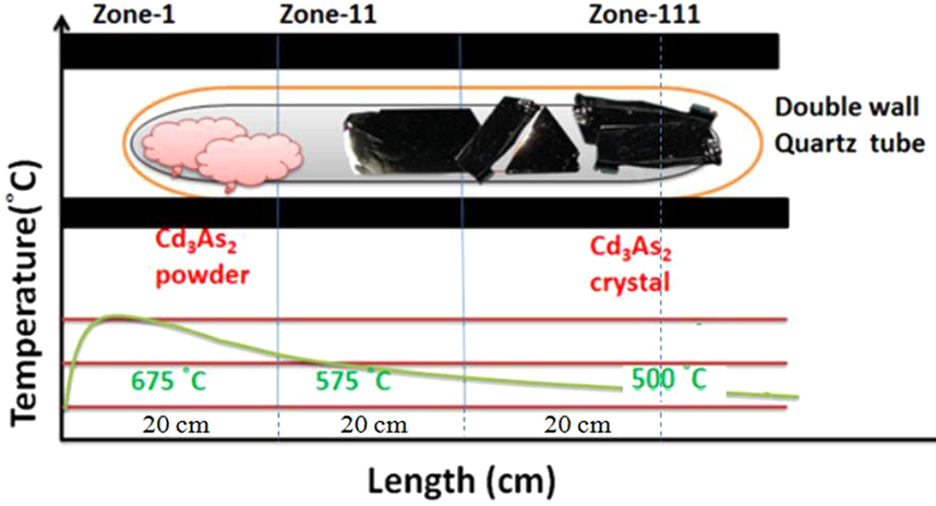
 Cadmium arsenide can be prepared as amorphous semiconductive
 glass
Glass is a non-crystalline, often transparent, amorphous solid that has widespread practical, technological, and decorative use in, for example, window panes, tableware, and optics. Glass is most often formed by rapid cooling ( quenching ...
. According to Hiscocks and Elliot, the preparation of cadmium arsenide was made from cadmium metal, which had a purity of 6 N from Kock-Light Laboratories Limited. Hoboken supplied β-arsenic with a purity of 99.999%. Stoichiometric proportions of the elements cadmium and arsenic were heated together. Separation was difficult and lengthy due to the ingot
An ingot is a piece of relatively pure material, usually metal, that is cast into a shape suitable for further processing. In steelmaking, it is the first step among semi-finished casting products. Ingots usually require a second procedure of sha ...
s sticking to the silica and breaking. Liquid encapsulated Stockbarger growth was created. Crystals are pulled from volatile melts in liquid encapsulation. The melt is covered by a layer of inert liquid, usually B2O3, and an inert gas pressure greater than the equilibrium vapor pressure is applied. This eliminates the evaporation from the melt which allows seeding and pulling to occur through the B2O3 layer.
Crystal structure
The unit cell of Cd3As2 is tetragonal. The arsenic ions are cubic close packed and the cadmium ions are tetrahedrally coordinated. The vacant tetrahedral sites provoked research by von Stackelberg and Paulus (1935), who determined the primary structure. Each arsenic ion is surrounded by cadmium ions at six of the eight corners of a distorted cube and the two vacant sites were at the diagonals. The crystalline structure of cadmium arsenide is very similar to that of zinc phosphide (Zn3P2), zinc arsenide (Zn3As2) and cadmium phosphide (Cd3P2). These compounds of the Zn-Cd-P-As quaternary system exhibit full continuous solid-solution.Nernst effect
Cadmium arsenide is used ininfrared detector
An infrared detector is a detector that reacts to infrared (IR) radiation. The two main types of detectors are thermal and photonic (photodetectors).
The thermal effects of the incident IR radiation can be followed through many temperature depen ...
s using the Nernst effect, and in thin-film dynamic pressure sensors. It can be also used to make magnetoresistors, and in photodetector
Photodetectors, also called photosensors, are sensors of light or other electromagnetic radiation. There is a wide variety of photodetectors which may be classified by mechanism of detection, such as photoelectric or photochemical effects, or ...
s.
Cadmium arsenide can be used as a dopant
A dopant, also called a doping agent, is a trace of impurity element that is introduced into a chemical material to alter its original electrical or optical properties. The amount of dopant necessary to cause changes is typically very low. When ...
for HgCdTe Hg1−xCdxTe or mercury cadmium telluride (also cadmium mercury telluride, MCT, MerCad Telluride, MerCadTel, MerCaT or CMT) is a chemical compound of cadmium telluride (CdTe) and mercury telluride (HgTe) with a tunable bandgap spanning the shortwav ...
.
References
External links
National Pollutant Inventory – Cadmium and compounds
{{Arsenides Arsenides Cadmium compounds II-V compounds