GeForce 9 Series on:
[Wikipedia]
[Google]
[Amazon]
The GeForce 9 series is the ninth generation of
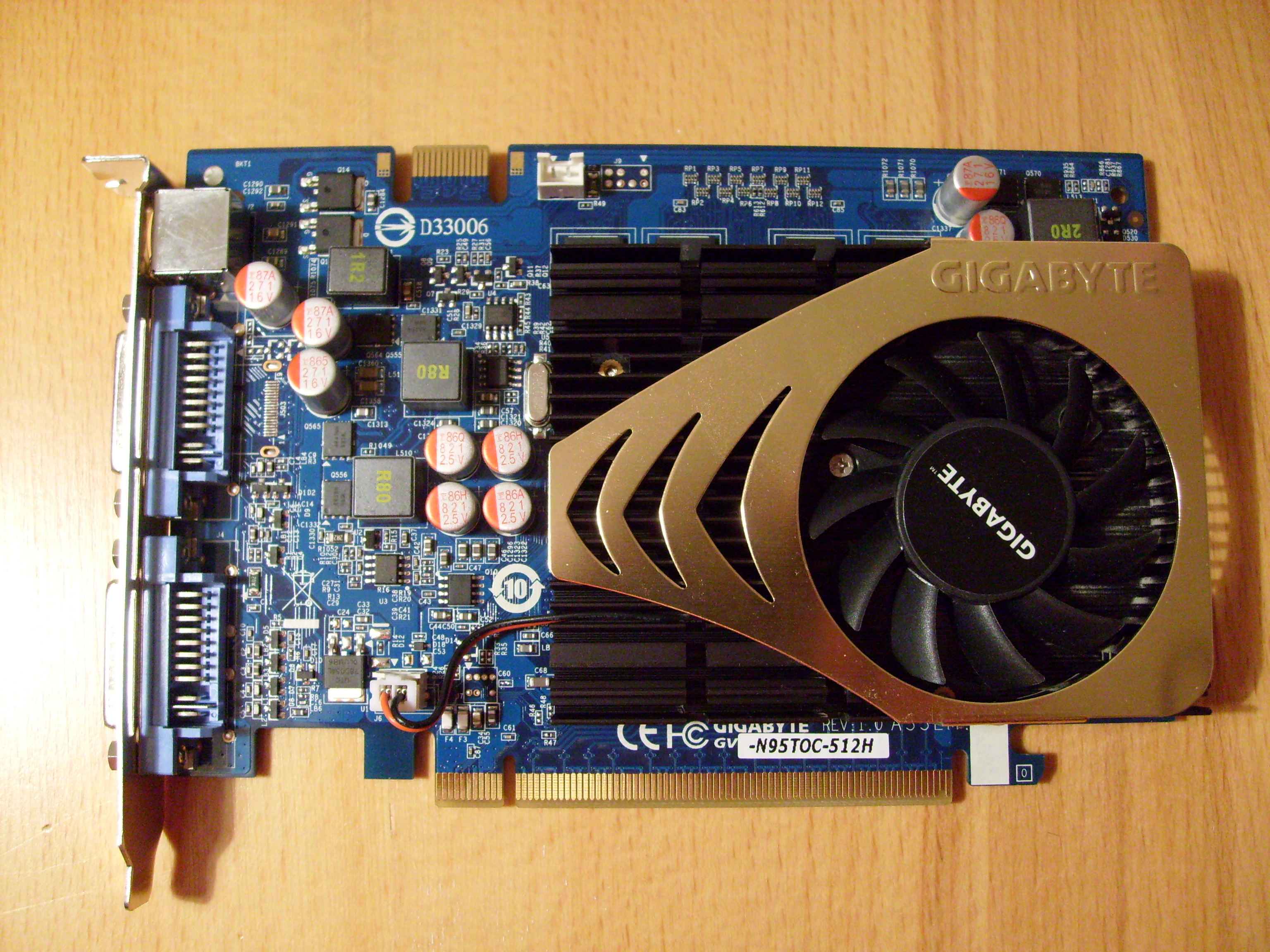
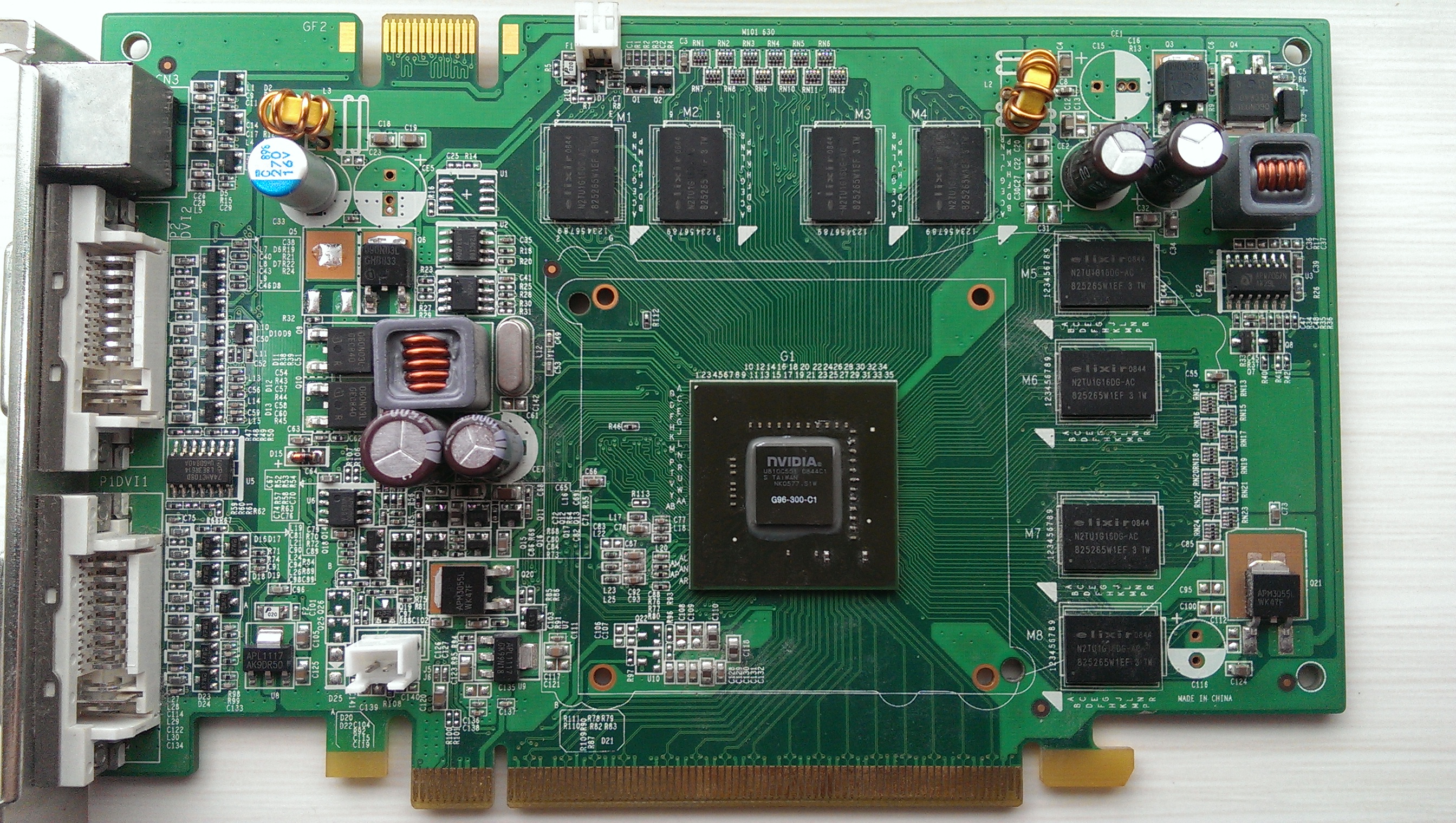 On July 29, 2008, the GeForce 9500 GT was officially launched.
*65 nm G96 GPU
*32 stream processors (32

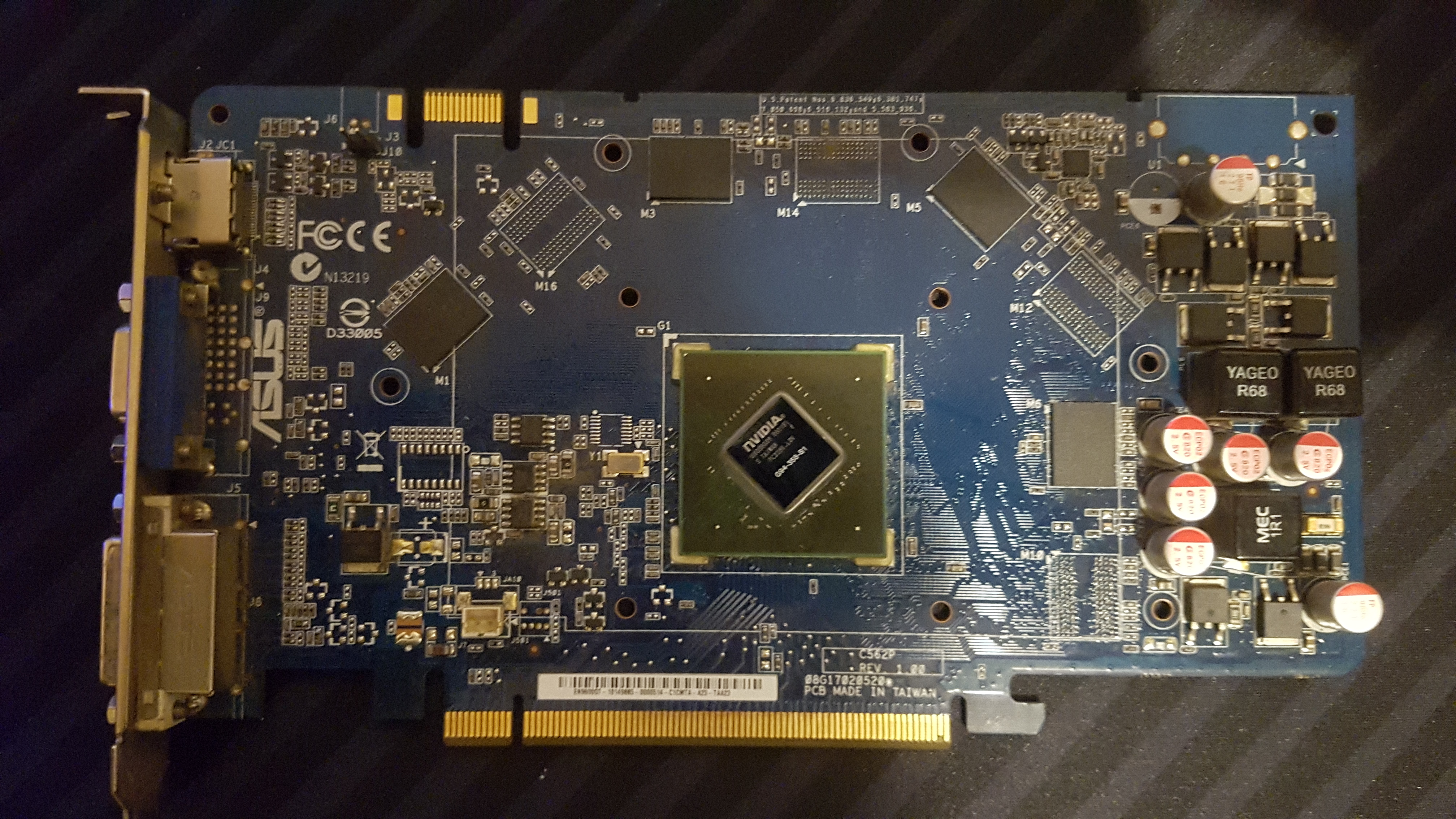
 On February 21, 2008, the GeForce 9600 GT was officially launched. It was an upgrade of 8600 GTS.
*65 nm G94 GPU
*64 stream processors
*16 raster operation (ROP) units, 32 texture address (TA) / texture filter (TF) units
*20.8 Gtexels/s fill rate
*650 MHz core clock, with a 1625 MHz unified shader clock
*1008 MHz memory (2016 MHz datarate), 256-bit interface for 64.5GB/s of bandwidth. (57.6 GB/s for 1800 MHz configuration)
*512–2048 MB of GDDR3 or DDR2 memory
*505M transistor count
*DirectX 10.0, Shader Model 4.0, OpenGL 2.1, and PCI-Express 2.0
*Supports second-generation PureVideo HD technology with partial VC1 decoding
*Is
 The GeForce 9600GS is a Hewlett Packard OEM card. It is based on a G94a core clocked at 500 MHz. It features 768 MB of DDR2 memory on a 192-bit bus.
"Hardware.no". (Accessed February 18, 2008 *256-bit memory interface *128 GB/s memory bandwidth *Release date: March 18, 2008 *Launch price of $666.99
EOL driver support for legacy products
/ref> * Windows XP 32-bit & Media Center Edition: version 340.52 released on July 29, 2014
Download
* Windows XP 64-bit: version 340.52 released on July 29, 2014
Download
* Windows Vista, 7, 8, 8.1 32-bit: version 342.01 (WHQL) released on December 14, 2016
Download
* Windows Vista, 7, 8, 8.1 64-bit: version 342.01 (WHQL) released on December 14, 2016
Download
* Windows 10, 32-bit: version 342.01 (WHQL) released on December 14, 2016
Download
* Windows 10, 64-bit: version 342.01 (WHQL) released on December 14, 2016
Download
GeForce 9800 GX2
Nvidia Nsight
{{DEFAULTSORT:Geforce 9 Series 9 Series Graphics cards Computer-related introductions in 2008
Nvidia
Nvidia CorporationOfficially written as NVIDIA and stylized in its logo as VIDIA with the lowercase "n" the same height as the uppercase "VIDIA"; formerly stylized as VIDIA with a large italicized lowercase "n" on products from the mid 1990s to ...
's GeForce
GeForce is a brand of graphics processing units (GPUs) designed by Nvidia. As of the GeForce 40 series, there have been eighteen iterations of the design. The first GeForce products were discrete GPUs designed for add-on graphics boards, inte ...
series of graphics processing unit
A graphics processing unit (GPU) is a specialized electronic circuit designed to manipulate and alter memory to accelerate the creation of images in a frame buffer intended for output to a display device. GPUs are used in embedded systems, m ...
s, the first of which was released on February 21, 2008. Products are based on a slightly repolished Tesla microarchitecture, adding PCIe
PCI Express (Peripheral Component Interconnect Express), officially abbreviated as PCIe or PCI-e, is a high-speed serial computer expansion bus standard, designed to replace the older PCI, PCI-X and AGP bus standards. It is the common ...
2.0 support, improved color and z-compression, and built on a 65 nm process, later using 55 nm process to reduce power consumption and die size ( GeForce 8 G8x GPUs only supported PCIe 1.1 and were built on 90 nm process or 80 nm process).
GeForce 9300 Series
Geforce 9100 G
* 65 nm G98 GPU * PCI-E x16 * 64-bit bus * 4 raster operations pipelines (ROP), 8 unified shaders * 540 MHz core clock * 256 MB DDR2, 400 MHz memory clock * 1300 MHz shader clock * 5.1 Gtexel
Texel (; Texels dialect: ) is a municipality and an island with a population of 13,643 in North Holland, Netherlands. It is the largest and most populated island of the West Frisian Islands in the Wadden Sea. The island is situated north of Den ...
s/s fill rate
* 7.6 GB/s memory bandwidth
* Supports DirectX 10, SM 4.0
* OpenGL 2.1 compliance
* Supports 1st generation PureVideo
PureVideo is Nvidia's hardware SIP core that performs video decoding. PureVideo is integrated into some of the Nvidia GPUs, and it supports hardware decoding of multiple video codec standards: MPEG-2, VC-1, H.264, HEVC, and AV1. PureVideo occu ...
HD technology with partial VC1 decoding
Geforce 9300 GS
On May 1, 2008, the GeForce 9300 GS was officially launched. * 80 nm G86 GPU * PCI-E x16 * 64-bit bus * 8 ROP, 16 unified shaders * 450 MHz core clock * 512 MB DDR2, 400 MHz memory clock * 900 MHz shader clock * 3.6 Gtexels/s fill rate * 6.4 GB/s memory bandwidth * Supports DirectX 10, SM 4.0 * OpenGL 2.1 complianceGeForce 9400 Series
GeForce 9400 GT
On August 27, 2008, the GeForce 9400 GT was officially launched. *65 nm G96 GPU *16 stream processors *550 MHz core, with a 1350 MHz unified shader clock *4.4 Gtexels/s fillrate *256/512/1024 MB 800 MHz DDR2 or 256 MB 1600 MHzGDDR3
GDDR3 SDRAM (Graphics Double Data Rate 3 SDRAM) is a type of DDR SDRAM specialized for graphics processing units (GPUs) offering less access latency and greater device bandwidths. Its specification was developed by ATI Technologies in collabor ...
, both with a 128-bit memory bus
*12.8 GB/s memory bandwidth for boards configured with DDR2 800 MHz memory
*Supports DirectX 10, Shader Model 4.0, OpenGL 3.3, and PCI-Express 2.0
*Supports 2nd generation PureVideo HD technology with partial VC1 decoding and HybridPower technology.
*Minimum of 300 watt power supply
GeForce 9500 Series
GeForce 9500 GT
 On July 29, 2008, the GeForce 9500 GT was officially launched.
*65 nm G96 GPU
*32 stream processors (32
 CUDA
CUDA (or Compute Unified Device Architecture) is a parallel computing platform and application programming interface (API) that allows software to use certain types of graphics processing units (GPUs) for general purpose processing, an approach ...
cores)
*4 multi processors (each multi processor has 8 cores)
*550 MHz core, with a 1400 MHz unified shader clock
*8.8 Gtexels/s fillrate
*256/512/1024 MB 1,600 MHz GDDR3
GDDR3 SDRAM (Graphics Double Data Rate 3 SDRAM) is a type of DDR SDRAM specialized for graphics processing units (GPUs) offering less access latency and greater device bandwidths. Its specification was developed by ATI Technologies in collabor ...
memory or 256 MB/512 MB 1,000 MHz GDDR2
Double Data Rate 2 Synchronous Dynamic Random-Access Memory (DDR2 SDRAM) is a double data rate (DDR) synchronous dynamic random-access memory (SDRAM) interface. It superseded the original DDR SDRAM specification, and was itself superseded by DDR3 ...
memory, both with a 128-bit memory bus
*25.6 GB/s memory bandwidth for boards configured with GDDR3 800 MHz memory
*Supports DirectX 10, Shader Model 4.0, OpenGL 3.3, and PCI-Express 2.0
*Supports 2nd generation PureVideo HD technology with partial VC1 decoding
*NVIDIA SLI-ready technology
*DVI support
GeForce 9500 GS
The 9500 GS is an OEM card that is based on the 9500 GT but geared towards the mainstream audience. *65 nm G96 GPU *32 stream processors *8 ROP units *550 MHz core, with a 1375 MHz defined unified shader clock *8.8 Gtexels/s fillrate *128/512 MB 1000 MHz DDR2 memory with a 128-bit memory bus *16.0 GB/s memory bandwidth *Supports DirectX 10, Shader Model 4.0, OpenGL 3.3, and PCI-Express 2.0 *Supports 2nd generation PureVideo HD technology with partial VC1 decoding *NVIDIA SLI-ready technology *DVI supportGeForce 9600 series
GeForce 9600 GT

 On February 21, 2008, the GeForce 9600 GT was officially launched. It was an upgrade of 8600 GTS.
*65 nm G94 GPU
*64 stream processors
*16 raster operation (ROP) units, 32 texture address (TA) / texture filter (TF) units
*20.8 Gtexels/s fill rate
*650 MHz core clock, with a 1625 MHz unified shader clock
*1008 MHz memory (2016 MHz datarate), 256-bit interface for 64.5GB/s of bandwidth. (57.6 GB/s for 1800 MHz configuration)
*512–2048 MB of GDDR3 or DDR2 memory
*505M transistor count
*DirectX 10.0, Shader Model 4.0, OpenGL 2.1, and PCI-Express 2.0
*Supports second-generation PureVideo HD technology with partial VC1 decoding
*Is
 HDCP
High-bandwidth Digital Content Protection (HDCP) is a form of digital copy protection developed by Intel Corporation to prevent copying of digital audio and video content as it travels across connections. Types of connections include DisplayPort ...
compatible, but its implementation depends on the manufacturer
*Supports CUDA
CUDA (or Compute Unified Device Architecture) is a parallel computing platform and application programming interface (API) that allows software to use certain types of graphics processing units (GPUs) for general purpose processing, an approach ...
and the Quantum Effects physics processing engine
*Almost double the performance of the previous Nvidia mid-range card, the GeForce 8600GTS
GeForce 9600 GS
 The GeForce 9600GS is a Hewlett Packard OEM card. It is based on a G94a core clocked at 500 MHz. It features 768 MB of DDR2 memory on a 192-bit bus.
GeForce 9600 GSO
The GeForce 9600 GSO was essentially a renamed 8800 GS. This tactic has been seen before in products such as the GeForce 7900 GTO to clear unsold stock when it is made obsolete by the next generation. Just like the 8800 GS, the 9600 GSO features 96 stream processors, a 550 MHz core clock with shaders clocked at 1,375 MHz, and either 384 or 768 MB of memory clocked at 800 MHz on a 192-bit memory bus. Some manufacturers have mistakenly listed some of their 768 MB models that have 96 stream processors as being based on the G94 chip, rather than the G92.GeForce 9600 GSO 512
After clearing the old 8800 GS stock, Nvidia revised the specification with a new core, and 512 MB of memory clocked at 900 MHz on a 256-bit bus. For these cards, the number of stream processors is halved to 48, with the core frequency increased to 650 MHz and the shader frequency increased to 1625 MHz. Some of these cards have 1024 megabytes of memory while still being a 512 model. The revised version is considered inferior in performance to the old version.GeForce 9600 GTX
XFX released a 9600 GTX based on the G92 chip featuring 96 stream processors, a 580 MHz core clock, 1450 MHz shaders and 512 MB of GDDR3 running at 1400 MHz on a 256-bit bus. Other than clock speeds, it is functionally the desktop equivalent version of the 9800M GT.GeForce 9800 Series
The GeForce 9800 series contains the GX2 (dual GPU), GTX, GTX+ and GT variants.GeForce 9800 GX2
On March 18, 2008, the GeForce 9800 GX2 was officially launched. The GeForce 9800 GX2 has the following specifications: *DualPCB
PCB may refer to:
Science and technology
* Polychlorinated biphenyl, an organic chlorine compound, now recognized as an environmental toxin and classified as a persistent organic pollutant
* Printed circuit board, a board used in electronics
* ...
s, dual GPU design
*197 W power consumption.
*Two 65nm
The 65 nm process is an advanced lithographic node used in volume CMOS ( MOSFET) semiconductor fabrication. Printed linewidths (i.e. transistor gate lengths) can reach as low as 25 nm on a nominally 65 nm process, while the pitc ...
process GPUs, with 256 total stream processors (128 per PCB).
*Supports Quad SLI
*Power of Two underclocked GeForce 8800 GTS 512 (G92) video cards in SLI Mode
*1 GiB
The byte is a unit of digital information that most commonly consists of eight bits. Historically, the byte was the number of bits used to encode a single character of text in a computer and for this reason it is the smallest addressable unit ...
(512 MiB per PCB) GDDR3 memory
*Supports DirectX 10, Shader Model 4, OpenGL 3.3, and PCI-Express 2.0
*Supports 2nd generation PureVideo HD technology with partial VC1 decoding
*Outputs include two DVI
Digital Visual Interface (DVI) is a video display interface developed by the Digital Display Working Group (DDWG). The digital interface is used to connect a video source, such as a video display controller, to a display device, such as a comp ...
ports, an HDMI
High-Definition Multimedia Interface (HDMI) is a proprietary audio/video interface for transmitting uncompressed video data and compressed or uncompressed digital audio data from an HDMI-compliant source device, such as a display controlle ...
output, and S/PDIF in connector on board for routing audio through the HDMI cable
*An 8-pin and a 6-pin power connector
*Clocks (Core/Shader/Memory): 600 MHz/1500 MHz/2000 MHz"NVIDIA GeForce 9800M GX2""Hardware.no". (Accessed February 18, 2008 *256-bit memory interface *128 GB/s memory bandwidth *Release date: March 18, 2008 *Launch price of $666.99
GeForce 9800 GTX
On April 1, 2008, the GeForce 9800 GTX was officially launched. Taken from an eVGA specification sheet: *128 CUDA cores *Clocks (Core/Shader/Memory): 675 MHz/1688 MHz/1100 MHz *256-bit memory interface *512 MB of GDDR3 memory *70.4 GB/s memory bandwidth *Texture Fill Rate of 43.2 (billion/s) *DirectX 10, Shader Model 4.0, OpenGL 3.3, and PCI-Express 2.0 *Supports 2nd generation PureVideo HD technology with partial VC1 decoding *Outputs include two DVI ports, an HDMI output (using Nvidia DVI to HDMI adapter (included)), and S/PDIF in connector on board for routing audio through the HDMI cable *Release date: 2008-04-01 *Launch Price of $349 In July 2008 Nvidia released a refresh of the 9800 GTX: the 9800 GTX+ (55 nm manufacturing process). It has faster core (738 MHz) and shader (1836 MHz) clocks. Since March 2009 this design is manufactured as GeForce GTS 250.GeForce 9800 GT
The 9800GT is identical to an 8800GT, although some were manufactured using a 55 nm technology instead of the 65 nm technology debuted on the 8800GT. The newer (55 nm) version supports HybridPower while the 65 nm version does not. ASUSTeK have released a 9800GT with Tri-SLI support. Taken from the Nvidia product detail page. *112 CUDA cores *512–1024 MB of GDDR3 memory *256-bit memory interface width *600 MHz graphics clock *1500 MHz processor clock *900 MHz memory clock *33.6 Gtexel/s texture fill rate *57.6 GB/s memory bandwidth *Supports DirectX 10, Shader Model 4.0, OpenGL 3.3, and PCI-Express 2.0 *Supports 2nd generation PureVideo HD technology with partial VC1 decodingTechnical Summary of Desktop G9x GPUs
*1 Unified shaders :Texture mapping unit
In computer graphics, a texture mapping unit (TMU) is a component in modern graphics processing units (GPUs). They are able to rotate, resize, and distort a bitmap image to be placed onto an arbitrary plane of a given 3D model as a texture, in a ...
s : Render output unit
In computer graphics, the render output unit (ROP) or raster operations pipeline is a hardware component in modern graphics processing units (GPUs) and one of the final steps in the rendering process of modern graphics cards. The pixel pipeline ...
s
Features
*Compute Capability: 1.1 has support for Atomic functions, which are used to write thread-safe programs.GeForce 9M Series
All graphical processing units in the GeForce 9M series feature: *Increased performance for similar power draw compared to GeForce 8M series for midrange and mid-high range notebooks *DirectX 10.0 and OpenGL 3.3 compatibility *16X antialiasing and PCI-Express 2.0 connectivity *Full HD DVD / Blu-ray hardware decoding9100M G
*1 TMU per pipeline *4 ROPs *8 stream processors *16 (v4.0) shader unified *26 GigaFLOPS *450 MHz core clock *1100 MHz shader clock *Integrated RAMDAC clock at 400 MHz *Memory clock depends on system memory *Up to 256 MB shared memory, 512 MB with Turbo Cache in Windows XP *64 bit memory interface (single-channel mode) / 128 bit memory interface (dual-channel mode) *Memory bandwidth depend on System Memory *1.8 Gtexels/s texture fill rate * (Specification based on Acer Aspire 4530 using EVEREST Ultimate Edition Version 4.60.1500PX and TechPowerUp GPU-Z v0.4.6)9200M GS
*8 stream processors *529 MHz core clock *1300 MHz shader clock *400 MHz memory clock *Up to 256 MB memory *64-bit memory interface *6.4 GB/s memory bandwidth *27.1 Gpixel/s pixel fill rate *4.2 Gtexel/s texture fill rate9300M G
*16 stream processors *400 MHz core clock *800 MHz shader clock *600 MHz memory clock *Up to 512 MB memory *64-bit memory interface *1.8 GB/s memory bandwidth *3.2 Gtexels/s texture fill rate9300M GS
*8 stream processors *580 MHz core clock *1450 MHz shader clock *800 MHz memory clock *Up to 512 MB memory *64-bit memory interface *6.9 GB/s memory bandwidth *4.6 Gtexels/s texture fill rate9400M G
*16 stream processors *Memory clock depends on system memory *64 bit memory interface (single-channel mode) / 128 bit memory interface (dual-channel mode) *Memory bandwidth depends on System Memory *3.6 Gtexels/s texture fill rate9500M G
*16 stream processors *500 MHz core clock *1250 MHz shader clock *800 MHz memory clock *Up to 1024 MB memory *128-bit memory interface *25.6 GB/s memory bandwidth *4.0 Gtexels/s texture fill rate9500M GS
*32 stream processors *475 MHz core clock *950 MHz shader clock *700 MHz memory clock *Up to 512 MB memory *128-bit memory interface *22.4 GB/s memory bandwidth *7.6 Gtexels/s texture fill rate9600M GS
*064A/8 core (G96) *32 stream processors *430 MHz core clock *1075 MHz shader clock *800/1600 MHz memory clock (effective) *Up to 1024 MB memory *128-bit memory interface *12.8 GB/s (with DDR2 type) or 25.6 GB/s (with GDDR3 type) memory bandwidth *6.8 Gtexels/s texture fill rate *103 GigaFLOPS9600M GT
*32 stream processors *500 MHz core clock *1250 MHz shader clock *800 MHz memory clock *Up to 1024 MB memory *128-bit memory interface *25.6 GB/s memory bandwidth *8.0 Gtexels/s texture fill rate9650M GT
*G96 core (65/55 nm) *32 stream processors *550 MHz core clock *1325 MHz shader clock *800 MHz memory clock *Up to 1024 MB memory *128 bit memory interface *25.6 GB/s memory bandwidth *8.8 Gtexels/s texture fill rate9700M GT
*G96 core *32 stream processors *625 MHz core clock *1550 MHz shader clock *800 MHz memory clock *128 bit memory interface *25.6 GB/s memory bandwidth *10.0 Gtexels/s texture fill rate *148.8 GigaFLOPS9700M GTS
*G94 core *48 stream processors *530 MHz core clock *1325 MHz shader clock *800 MHz memory clock *256 bit memory interface *51.2 GB/s memory bandwidth *12.7 Gtexels/s texture fill rate *190.8 GigaFLOPS9800M GS
*G94 core *64 stream processors *530 MHz core clock *1325 MHz shader clock *800 MHz memory clock *256 bit memory interface *51.2 GB/s memory bandwidth *17.0 Gtexels/s texture fill rate *254 GigaFLOPS9800M GTS
*G94 core *64 stream processors *600 MHz core clock *1500 MHz shader clock *800 MHz memory clock *256 bit memory interface *51.2 GB/s memory bandwidth *19.2 Gtexels/s texture fill rate *288 GigaFLOPS9800M GT
*G94 core *96 stream processors *500 MHz core clock *1250 MHz shader clock *800 MHz memory clock *256 bit memory interface *51.2 GB/s memory bandwidth *24.0 Gtexels/s texture fill rate *360 GigaFLOPS9800M GTX
*G92 core *112 stream processors *500 MHz core clock *1250 MHz shader clock *800 MHz memory clock *256 bit memory interface *51.2 GB/s memory bandwidth *28.0 Gtexels/s texture fill rate *420 GigaFLOPSTechnical summary
Discontinued support
NVIDIA has ceased driver support for GeForce 9 series on April 1, 2016./ref> * Windows XP 32-bit & Media Center Edition: version 340.52 released on July 29, 2014
Download
* Windows XP 64-bit: version 340.52 released on July 29, 2014
Download
* Windows Vista, 7, 8, 8.1 32-bit: version 342.01 (WHQL) released on December 14, 2016
Download
* Windows Vista, 7, 8, 8.1 64-bit: version 342.01 (WHQL) released on December 14, 2016
Download
* Windows 10, 32-bit: version 342.01 (WHQL) released on December 14, 2016
Download
* Windows 10, 64-bit: version 342.01 (WHQL) released on December 14, 2016
Download
See also
*Comparison of Nvidia graphics processing units
This list contains general information about graphics processing units (GPUs) and video cards from Nvidia, based on official specifications. In addition some Nvidia motherboards come with integrated onboard GPUs. Limited/Special/Collectors' Editio ...
* GeForce 8 series
* GeForce 100 series
The GeForce 100 series is a series of Tesla-based graphics processing units developed by Nvidia, first released in March 2009. Its cards are rebrands of GeForce 9 series cards, available only for OEMs. However, the GTS 150 was briefly available ...
* GeForce 200 series
The GeForce 200 series is a series of Tesla-based GeForce graphics processing units developed by Nvidia.
Architecture
The GeForce 200 Series introduced Nvidia's second generation of Tesla (microarchitecture), Nvidia's unified shader architec ...
* GeForce 300 series
The GeForce 300 series is a series of Tesla-based graphics processing units developed by Nvidia, first released in November 2009. Its cards are rebrands of the GeForce 200 series cards, available only for OEMs. All GPUs of the series support D ...
* Nvidia Quadro
Quadro was Nvidia's brand for graphics cards intended for use in workstations running professional computer-aided design (CAD), computer-generated imagery (CGI), digital content creation (DCC) applications, scientific calculations and machine l ...
NVIDIA's workstation graphics solution
* Nvidia Tesla
Nvidia Tesla was the name of Nvidia's line of products targeted at stream processing or general-purpose graphics processing units (GPGPU), named after pioneering electrical engineer Nikola Tesla. Its products began using GPUs from the G80 seri ...
NVIDIA's first dedicated general purpose GPU (graphical processor unit)
References
External links
GeForce 9800 GX2
Nvidia Nsight
{{DEFAULTSORT:Geforce 9 Series 9 Series Graphics cards Computer-related introductions in 2008