Electron-hole Recombination
   HOME

TheInfoList


OR:

In the solid-state physics of semiconductors, carrier generation and carrier recombination are processes by which mobile charge carriers (electrons and electron holes) are created and eliminated. Carrier generation and recombination processes are fundamental to the operation of many optoelectronics, optoelectronic semiconductor devices, such as photodiodes, light-emitting diodes and laser diodes. They are also critical to a full analysis of p-n junction devices such as bipolar junction transistors and p-n junction diodes. The electron–hole pair is the fundamental unit of generation and recombination in Semiconductor, inorganic semiconductors, corresponding to an electron transitioning between the valence band and the conduction band where generation of electron is a transition from the valence band to the conduction band and recombination leads to a reverse transition.


Overview

Like other solids, semiconductor materials have an electronic band structure determined by the crystal properties of the material. Energy distribution among electrons is described by the Fermi level and the temperature of the electrons. At absolute zero temperature, all of the electrons have energy below the Fermi level; but at non-zero temperatures the energy levels are filled following a Fermi-Dirac distribution. In undoped semiconductors the Fermi level lies in the middle of a ''forbidden band'' or band gap between two ''allowed bands'' called the ''valence band'' and the ''conduction band''. The valence band, immediately below the forbidden band, is normally very nearly completely occupied. The conduction band, above the Fermi level, is normally nearly completely empty. Because the valence band is so nearly full, its electrons are not mobile, and cannot flow as electric current. However, if an electron in the valence band acquires enough energy to reach the conduction band (as a result of interaction with other electrons, Electron hole, holes, photons, or the Phonon, vibrating crystal lattice itself), it can flow freely among the nearly empty conduction band energy states. Furthermore, it will also leave behind a hole that can flow as current exactly like a physical charged particle. Carrier generation describes processes by which electrons gain energy and move from the valence band to the conduction band, producing two mobile carriers; while recombination describes processes by which a conduction band electron loses energy and re-occupies the energy state of an electron hole in the valence band. These processes must conserve both quantized energy and crystal momentum, and the Phonon, vibrating lattice plays a large role in conserving momentum as, in collisions, photons can transfer very little momentum in relation to their energy.


Relation between generation and recombination
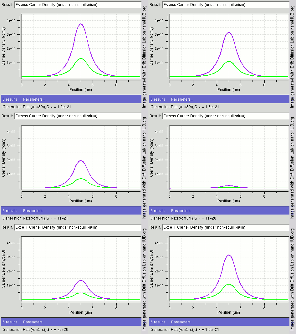
Recombination and generation are always happening in semiconductors, both optically and thermally. As predicted by thermodynamics, a material at thermal equilibrium will have generation and recombination rates that are balanced so that the net charge carrier density remains constant. The resulting probability of occupation of energy states in each energy band is given by Fermi–Dirac statistics. The product of the Charge carrier density, electron and hole densities (n and p) is a constant (n_o p_o=n_i^2) at equilibrium, maintained by recombination and generation occurring at equal rates. When there is a surplus of carriers (i.e., n p>n_i^2), the rate of recombination becomes greater than the rate of generation, driving the system back towards equilibrium. Likewise, when there is a deficit of carriers (i.e., n p), the generation rate becomes greater than the recombination rate, again driving the system back towards equilibrium. As the electron moves from one energy band to another, the energy and momentum that it has lost or gained must go to or come from the other particles involved in the process (e.g. photons, electron, or the Phonon, system of vibrating lattice atoms).


Carrier generation

When light interacts with a material, it can either be absorption (electromagnetic radiation), absorbed (generating a pair of free carriers or an exciton) or it can ''stimulate'' a recombination event. The generated photon has similar properties to the one responsible for the event. Absorption is the active process in photodiodes, solar cells and other semiconductor photodetectors, while stimulated emission is the principle of operation in laser diodes. Besides light excitation, carriers in semiconductors can also be generated by an external electric field, for example in light-emitting diodes and transistors. When light with sufficient energy hits a semiconductor, it can excite electrons across the band gap. This generates additional charge carriers, temporarily lowering the electrical resistance of materials. This higher conductivity in the presence of light is known as photoconductivity. This conversion of light into electricity is widely used in photodiodes.


Recombination mechanisms

Carrier recombination can happen through multiple relaxation channels. The main ones are band-to-band recombination, Shockley–Read–Hall (SRH) trap-assisted recombination, Auger recombination and surface recombination. These decay channels can be separated into radiative and non-radiative. The latter occurs when the excess energy is converted into heat by phonon emission after the mean lifetime \tau_, whereas in the former at least part of the energy is released by light emission or luminescence after a radiative lifetime \tau_. The carrier lifetime \tau is then obtained from the rate of both type of events according to: \frac=\frac+\frac From which we can also define the internal quantum efficiency or quantum yield, \eta as: \eta = \frac =\frac \leq 1.


Radiative recombination


Band-to-band radiative recombination

''Band-to-band recombination'' is the name for the process of electrons jumping down from the conduction band to the valence band in a radiative manner. During band-to-band recombination, a form of spontaneous emission, the energy absorbed by a material is released in the form of photons. Generally these photons contain the same or stokes shift, less energy than those initially absorbed. This effect is how light-emitting diode, LEDs create light. Because the photon carries relatively little momentum, radiative recombination is significant only in direct bandgap materials. This process is also known as ''bimolecular recombination'.'' This type of recombination depends on the density of electrons and holes in the excited state, denoted by n(t) and p(t) respectively. Let us represent the radiative recombination as R_r and the carrier generation rate as G. Total generation is the sum of thermal generation G0 and generation due to light shining on the semiconductor GL: G = G_0 + G_L Here we will consider the case in which there is no illumination on the semiconductor. Therefore G_L = 0 and G = G_0 , and we can express the change in carrier density as a function of time as = G-R_r = G_0 - R_r Because the rate of recombination is affected by both the concentration of free electrons and the concentration of holes that are available to them, we know that Rr should be proportional to np: R_r \propto np and we add a proportionality constant Br to eliminate the \propto sign: R_r=B_r np If the semiconductor is in thermal equilibrium, the rate at which electrons and holes recombine must be balanced by the rate at which they are generated by the spontaneous transition of an electron from the valence band to the conduction band. The recombination rate R_0 must be exactly balanced by the thermal generation rate G_0. Therefore: R_0 = G_0 = B_r n_0 p_0 where n_0 and p_0 are the equilibrium carrier densities. Using the Mass action law (electronics), mass action law np=n_i^2,with n_i being the intrinsic carrier density, we can rewrite it as R_0 = G_0 = B_r n_0 p_0= B_r n_i^2 The non-equilibrium carrier densities are given by n= n_0+ \Delta n, p= p_0+ \Delta p Then the new recombination rate R_\text becomes, R_\text = R_r-G_0 = B_rnp-G_0 = B_r(n_0 + \Delta n)(p_0 + \Delta p)-G_0 Because n_0 \gg\Delta n and p_0 \gg \Delta p, we can say that \Delta n\Delta p \approx 0 R_\text= B_r(n_0 + \Delta n)(p_0 + \Delta p)-G_0 = B_r(n_0p_0 + \Delta n p_0 +\Delta p n_0) - B_r n_i^2 R_\text= B_r(n_i^2 + \Delta n p_0 +\Delta p n_0- n_i^2) R_\text= B_r(\Delta n p_0 +\Delta p n_0) In an n-type semiconductor, p_0 \ll n_0 and \Delta p \ll n_0 thus R_ \approx B_r\Delta p n_0 Net recombination is the rate at which excess holes \Delta p disappear \frac = - R_\text \approx - B_r\Delta p n_0 Solve this differential equation to get a standard exponential decay \Delta p = p_e^ where pmax is the maximum excess hole concentration when t = 0. (It can be proved that p_=\frac, but here we will not discuss that). When t = \frac, all of the excess holes will have disappeared. Therefore, we can define the lifetime of the excess holes in the material \tau_p = \frac So the lifetime of the minority carrier is dependent upon the majority carrier concentration.


Stimulated emission

''Stimulated emission'' is a process in which an incident photon interacts with an excited electron causing it to recombine and emit a photon with the same properties of the incident one, in terms of phase (waves), phase, frequency, Polarization (waves), polarization, and Direction (geometry), direction of travel. Stimulated emission together with the principle of population inversion are at the heart of operation of lasers and masers. It has been shown by Einstein coefficients, Einstein at the beginning of the twentieth century that if the excited and the ground level are Degeneracy (quantum mechanics), non degenerate then the absorption rate W_and the stimulated emission rate W_are the same. Else if level 1 and level 2 are g_1-fold and g_2-fold degenerate respectively, the new relation is:g_1 W_= g_2 W_.


Trap emission

''Trap emission'' is a multistep process wherein a carrier falls into defect-related wavestates in the middle of the bandgap. A ''trap'' is a defect capable of holding a carrier. The trap emission process recombines electrons with holes and emits photons to conserve energy. Due to the multistep nature of trap emission, a phonon is also often emitted. Trap emission can proceed by use of bulk defects or surface defects.


Non-radiative recombination

Non-radiative recombination is a process in phosphors and semiconductors, whereby charge carriers recombine releasing phonons instead of photons. Non-radiative recombination in optoelectronics and phosphors is an unwanted process, lowering the light generation efficiency and increasing heat losses. Non-radiative life time is the average time before an electron in the conduction band of a semiconductor recombines with a electron hole, hole. It is an important parameter in optoelectronics where radiative recombination is required to produce a photon; if the non-radiative life time is shorter than the radiative, a carrier is more likely to recombine non-radiatively. This results in low internal quantum efficiency.


Shockley–Read–Hall (SRH)

In ''Shockley-Read-Hall recombination'' (''SRH''), also called ''trap-assisted recombination'', the electron in transition between electronic band structure, bands passes through a new energy state (localized state) created within the band gap by a dopant or a Crystal defect, defect in the crystal lattice; such energy states are called ''traps''. Non-radiative recombination occurs primarily at such sites. The energy is exchanged in the form of lattice vibration, a phonon exchanging thermal energy with the material. Since traps can absorb differences in momentum between the carriers, SRH is the dominant recombination process in silicon and other direct and indirect band gaps, indirect bandgap materials. However, trap-assisted recombination can also dominate in direct and indirect band gaps, direct bandgap materials under conditions of very low charge carrier density, carrier densities (very low level injection) or in materials with high density of traps such as Perovskite solar cell, perovskites. The process is named after William Shockley, William Thornton Read and Robert N. Hall, who published it in 1952.


Types of traps


= Electron traps vs. hole traps

= Even though all the recombination events can be described in terms of electron movements, it is common to visualize the different processes in terms of excited electron and the electron ''holes'' they leave behind. In this context, if trap levels are close to the conduction band, they can temporarily immobilize excited electrons or in other words, they are ''electron traps''. On the other hand, if their energy lies close to the valence band they become ''hole traps.''


=Shallow traps vs. deep traps

= The distinction between shallow and deep traps is commonly made depending on how close electron traps are to the conduction band and how close hole traps are to the valence band. If the difference between trap and band is smaller than the kT (energy), thermal energy kBT it is often said that it is a ''shallow trap''. Alternatively, if the difference is larger than the thermal energy, it is called a Deep-level trap, deep trap. This difference is useful because shallow traps can be emptied more easily and thus are often not as detrimental to the performance of optoelectronic devices.


SRH model

In the SRH model, four things can happen involving trap levels: * An electron in the conduction band can be trapped in an intragap state. * An electron can be emitted into the conduction band from a trap level. * A hole in the valence band can be captured by a trap. This is analogous to a filled trap releasing an electron into the valence band. * A captured hole can be released into the valence band. Analogous to the capture of an electron from the valence band. When carrier recombination occurs through traps, we can replace the valence density of states by that of the intragap state. The term p(n)is replaced by the density of trapped electrons/holes N_t(1-f_t). R_=B_n n N_t (1-f_t) Where N_t is the density of trap states and f_t is the probability of that occupied state. Considering a material containing both types of traps, we can define two trapping coefficients B_n, B_p and two de-trapping coefficients G_n, G_p. In equilibrium, both trapping and de-trapping should be balanced and R_=G_). Then, the four rates as a function of f_tbecome: \begin R_=B_nnN_(1-f_t)& G_n=B_n n_t N_t f_t \\ R_=B_p p N_t f_t&G_p=B_p p_t N_t (1-f_t) \end Where n_t and p_t are the electron and hole densities when the quasi Fermi level matches the trap energy. In steady-state condition, the net recombination rate of electrons should match the net recombination rate for holes, in other words: R_-G_n =R_-G_p. This eliminates the occupation probability f_t and leads to the Shockley-Read-Hall expression for the trap-assisted recombination: R=\frac Where the average lifetime for electrons and holes are defined as: \tau_n=\frac,\quad \tau_p=\frac.


Auger recombination

In ''Auger recombination'' the energy is given to a third carrier which is excited to a higher energy level without moving to another energy band. After the interaction, the third carrier normally loses its excess energy to thermal vibrations. Since this process is a three-particle interaction, it is normally only significant in non-equilibrium conditions when the carrier density is very high. The Auger effect process is not easily produced, because the third particle would have to begin the process in the unstable high-energy state. In thermal equilibrium the Auger recombination R_A and thermal generation rate G_0 equal each other R_ = G_0 = C_n n_0^2 p_0 + C_p n_0 p_0^2 where C_n,C_p are the Auger capture probabilities. The non-equilibrium Auger recombination rate r_A and resulting net recombination rate U_A under steady-state conditions are r_A = C_n n^2 p + C_p n p^2 \,, \quad R_A = r_A-G_0 = C_n \left( n^2p-n_0^2 p_0 \right) + C_p \left( np^2- n_0 p_0^2 \right) \,. The Auger lifetime \tau_A is given by \tau_A = \frac = \frac \,. The mechanism causing Light-emitting diode#Efficiency drop, LED efficiency drop was identified in 2007 as Auger recombination, which met with a mixed reaction.Stevenson, Richard (August 2009
"The LED's Dark Secret: Solid-state lighting won't supplant the lightbulb until it can overcome the mysterious malady known as droop"
IEEE Spectrum
In 2013, an experimental study claimed to have identified Auger recombination as the cause of efficiency droop. However, it remains disputed whether the amount of Auger loss found in this study is sufficient to explain the droop. Other frequently quoted evidence against Auger as the main droop-causing mechanism is the low-temperature dependence of this mechanism, which is the opposite of that found for the drop.


Surface recombination

Trap-assisted recombination at the surface of a semiconductor is referred to as surface recombination. This occurs when traps at or near the surface or interface of the semiconductor form due to dangling bonds caused by the sudden discontinuation of the semiconductor crystal. Surface recombination is characterized by surface recombination velocity which depends on the density of surface defects. In applications such as solar cells, surface recombination may be the dominant mechanism of recombination due to the collection and extraction of free carriers at the surface. In some applications of solar cells, a layer of transparent material with a large band gap, also known as a window layer, is used to minimize surface recombination. Passivation (chemistry), Passivation techniques are also employed to minimize surface recombination.


Langevin recombination

For free carriers in low-mobility systems, the recombination rate is often described with the Langevin recombination rate. The model is often used for disordered systems such as organic materials (and is hence relevant for organic solar cells) and other such systems. The Langevin recombination strength is defined as \gamma = \tfrac\mu.


See also

* Cage effect * Auger effect


References

{{reflist, 30em


Further reading

* N.W. Ashcroft and N.D. Mermin, ''Solid State Physics'', Brooks Cole, 1976


External links


PV Lighthouse Recombination Calculator

PV Lighthouse Band Gap CalculatorPV Education
Semiconductors Optoelectronics Charge carriers