|
Plumbene
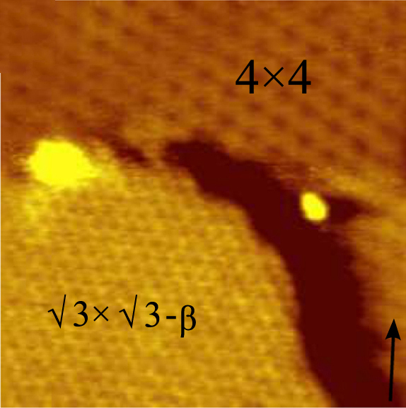
Plumbene is a material made up of a single layer of lead atoms. The material is created in a process similar to that of graphene, silicene, germanene, and stanene, in which high vacuum and high temperature are used to deposit a layer of lead atoms on a substrate. High-quality thin films of plumbene have revealed two-dimensional honeycomb structures. First researched by Indian scientists, further investigations are being done around the world. Preparation and structure In April 2019, J. Yuhara and others reported the deposition of a single atom thickness by molecular beam epitaxy with a segregation method upon a palladium surface in a crystal lattice with Miller indices (111). The structure was confirmed with scanning tunneling microscopy (STM) revealing a nearly flat honeycomb structure. There is no evidence of any three-dimensional islands, but one notices a unique nanostructured tessellation all over the terraces looking like a space-filling polyhedral foam reduced to dimension 2. ... [...More Info...] [...Related Items...] OR: [Wikipedia] [Google] [Baidu] |
Graphene
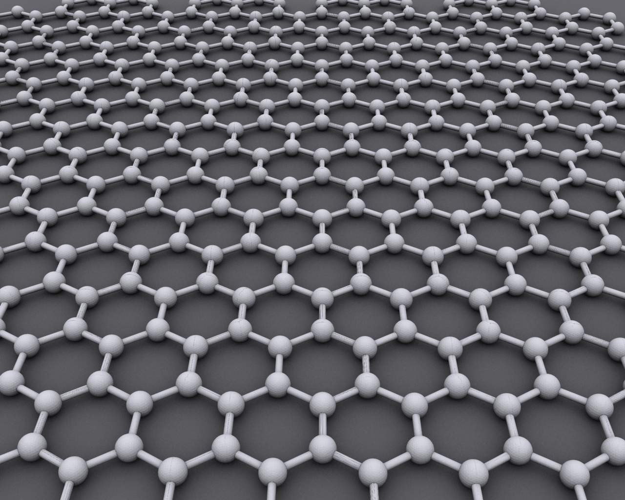
Graphene () is an allotrope of carbon consisting of a single layer of atoms arranged in a hexagonal lattice nanostructure. "Carbon nanostructures for electromagnetic shielding applications", Mohammed Arif Poothanari, Sabu Thomas, et al., ''Industrial Applications of Nanomaterials'', 2019. "Carbon nanostructures include various low-dimensional allotropes of carbon including carbon black (CB), carbon fiber, carbon nanotubes (CNTs), fullerene, and graphene." The name is derived from "graphite" and the suffix -ene, reflecting the fact that the allotrope of carbon contains numerous double bonds. Each atom in a graphene sheet is connecte ... [...More Info...] [...Related Items...] OR: [Wikipedia] [Google] [Baidu] |
Silicene
Silicene is a two-dimensional allotrope of silicon, with a hexagonal honeycomb structure similar to that of graphene. Contrary to graphene, silicene is not flat, but has a periodically buckled topology; the coupling between layers in silicene is much stronger than in multilayered graphene; and the oxidized form of silicene, 2D silica, has a very different chemical structure from graphene oxide. History Although theorists had speculated about the existence and possible properties of free-standing silicene, researchers first observed silicon structures that were suggestive of silicene in 2010. Using a scanning tunneling microscope they studied self-assembled silicene nanoribbons and silicene sheets deposited onto a silver crystal, Ag(110) and Ag(111), with atomic resolution. The images revealed hexagons in a honeycomb structure similar to that of graphene, which, however, were shown to originate from the silver surface mimicking the hexagons. Density functional theory (DFT) cal ... [...More Info...] [...Related Items...] OR: [Wikipedia] [Google] [Baidu] |
Germanene
Germanene is a material made up of a single layer of germanium atoms. The material is created in a process similar to that of silicene and graphene, in which high vacuum and high temperature are used to deposit a layer of germanium atoms on a substrate. High-quality thin films of germanene have revealed unusual two-dimensional structures with novel electronic properties suitable for semiconductor device applications and materials science research. Preparation and structure In September 2014, G. Le Lay and others reported the deposition of a single atom thickness, ordered and two-dimensional multi-phase film by molecular beam epitaxy upon a gold surface in a crystal lattice with Miller indices (111). The structure was confirmed with scanning tunneling microscopy (STM) revealing a nearly flat honeycomb structure. Additional confirmation was obtained by spectroscopic measurement and density functional theory calculations. The development of high quality and nearly flat single atom ... [...More Info...] [...Related Items...] OR: [Wikipedia] [Google] [Baidu] |
Lead
Lead is a chemical element with the symbol Pb (from the Latin ) and atomic number 82. It is a heavy metal that is denser than most common materials. Lead is soft and malleable, and also has a relatively low melting point. When freshly cut, lead is a shiny gray with a hint of blue. It tarnishes to a dull gray color when exposed to air. Lead has the highest atomic number of any stable element and three of its isotopes are endpoints of major nuclear decay chains of heavier elements. Lead is toxic, even in small amounts, especially to children. Lead is a relatively unreactive post-transition metal. Its weak metallic character is illustrated by its amphoteric nature; lead and lead oxides react with acids and bases, and it tends to form covalent bonds. Compounds of lead are usually found in the +2 oxidation state rather than the +4 state common with lighter members of the carbon group. Exceptions are mostly limited to organolead compounds. Like the lighter members of the ... [...More Info...] [...Related Items...] OR: [Wikipedia] [Google] [Baidu] |
Nature (journal)
''Nature'' is a British weekly scientific journal founded and based in London, England. As a multidisciplinary publication, ''Nature'' features peer-reviewed research from a variety of academic disciplines, mainly in science and technology. It has core editorial offices across the United States, continental Europe, and Asia under the international scientific publishing company Springer Nature. ''Nature'' was one of the world's most cited scientific journals by the Science Edition of the 2019 ''Journal Citation Reports'' (with an ascribed impact factor of 42.778), making it one of the world's most-read and most prestigious academic journals. , it claimed an online readership of about three million unique readers per month. Founded in autumn 1869, ''Nature'' was first circulated by Norman Lockyer and Alexander Macmillan as a public forum for scientific innovations. The mid-20th century facilitated an editorial expansion for the journal; ''Nature'' redoubled its efforts in exp ... [...More Info...] [...Related Items...] OR: [Wikipedia] [Google] [Baidu] |
Stanene
Stanene is a topological insulator, theoretically predicted by Prof. Shoucheng Zhang's group at Stanford, which may display dissipationless currents at its edges near room temperature. It is composed of tin atoms arranged in a single layer, in a manner similar to graphene. Stanene got its name by combining ''stannum'' (the List of chemical element name etymologies, Latin name for tin) with the suffix ''-ene'' used by graphene. Research is ongoing in Germany and China, as well as at laboratories at Stanford and UCLA. The addition of fluorine atoms to the tin lattice could extend the critical temperature up to 100 °C. This would make it practical for use in integrated circuits to make smaller, faster and more energy efficient computers. See also *Graphene *Silicene Silicene is a two-dimensional allotrope of silicon, with a hexagonal honeycomb structure similar to that of graphene. Contrary to graphene, silicene is not flat, but has a periodically buckled topology; the cou ... [...More Info...] [...Related Items...] OR: [Wikipedia] [Google] [Baidu] |
Molecular Beam Epitaxy
Molecular-beam epitaxy (MBE) is an epitaxy method for thin-film deposition of single crystals. MBE is widely used in the manufacture of semiconductor devices, including transistors, and it is considered one of the fundamental tools for the development of nanotechnologies. MBE is used to fabricate diodes and MOSFETs (MOS field-effect transistors) at microwave frequencies, and to manufacture the lasers used to read optical discs (such as CDs and DVDs). History Original ideas of MBE process were first established by Günther. Films he deposited were not epitaxial, but were deposited on glass substrates. With the development of vacuum technology, MBE process was demonstrated by Davey and Pankey who succeeded in growing GaAs epitaxial films on single crystal GaAs substrates using Günther's method. Major subsequent development of MBE films was enabled by J.R. Arthur's investigations of kinetic behavior of growth mechanisms and Alfred Y. Cho's in situ observation of MBE process usi ... [...More Info...] [...Related Items...] OR: [Wikipedia] [Google] [Baidu] |
Palladium
Palladium is a chemical element with the symbol Pd and atomic number 46. It is a rare and lustrous silvery-white metal discovered in 1803 by the English chemist William Hyde Wollaston. He named it after the asteroid Pallas, which was itself named after the epithet of the Greek goddess Athena, acquired by her when she slew Pallas. Palladium, platinum, rhodium, ruthenium, iridium and osmium form a group of elements referred to as the platinum group metals (PGMs). They have similar chemical properties, but palladium has the lowest melting point and is the least dense of them. More than half the supply of palladium and its congener platinum is used in catalytic converters, which convert as much as 90% of the harmful gases in automobile exhaust (hydrocarbons, carbon monoxide, and nitrogen dioxide) into nontoxic substances (nitrogen, carbon dioxide and water vapor). Palladium is also used in electronics, dentistry, medicine, hydrogen purification, chemical applications, groundwate ... [...More Info...] [...Related Items...] OR: [Wikipedia] [Google] [Baidu] |
Crystal Lattice
In geometry and crystallography, a Bravais lattice, named after , is an infinite array of discrete points generated by a set of discrete translation operations described in three dimensional space by : \mathbf = n_1 \mathbf_1 + n_2 \mathbf_2 + n_3 \mathbf_3, where the ''ni'' are any integers, and a''i'' are ''primitive translation vectors'', or ''primitive vectors'', which lie in different directions (not necessarily mutually perpendicular) and span the lattice. The choice of primitive vectors for a given Bravais lattice is not unique. A fundamental aspect of any Bravais lattice is that, for any choice of direction, the lattice appears exactly the same from each of the discrete lattice points when looking in that chosen direction. The Bravais lattice concept is used to formally define a ''crystalline arrangement'' and its (finite) frontiers. A crystal is made up of one or more atoms, called the ''basis'' or ''motif'', at each lattice point. The ''basis'' may consist of atoms, mo ... [...More Info...] [...Related Items...] OR: [Wikipedia] [Google] [Baidu] |
Miller Indices
Miller indices form a notation system in crystallography for lattice planes in crystal (Bravais) lattices. In particular, a family of lattice planes of a given (direct) Bravais lattice is determined by three integers ''h'', ''k'', and ''ℓ'', the ''Miller indices''. They are written (hkℓ), and denote the family of (parallel) lattice planes (of the given Bravais lattice) orthogonal to \mathbf_ = h\mathbf + k\mathbf + \ell\mathbf, where \mathbf are the basis or primitive translation vectors of the reciprocal lattice for the given Bravais lattice. (Note that the plane is not always orthogonal to the linear combination of direct or original lattice vectors h\mathbf + k\mathbf + \ell\mathbf because the direct lattice vectors need not be mutually orthogonal.) This is based on the fact that a reciprocal lattice vector \mathbf (the vector indicating a reciprocal lattice point from the reciprocal lattice origin) is the wavevector of a plane wave in the Fourier series of a spatia ... [...More Info...] [...Related Items...] OR: [Wikipedia] [Google] [Baidu] |
Scanning Tunneling Microscopy
A scanning tunneling microscope (STM) is a type of microscope used for imaging surfaces at the atomic level. Its development in 1981 earned its inventors, Gerd Binnig and Heinrich Rohrer, then at IBM Zürich, the Nobel Prize in Physics in 1986. STM senses the surface by using an extremely sharp conducting tip that can distinguish features smaller than 0.1 nm with a 0.01 nm (10 pm) depth resolution. This means that individual atoms can routinely be imaged and manipulated. Most microscopes are built for use in ultra-high vacuum at temperatures approaching zero kelvin, but variants exist for studies in air, water and other environments, and for temperatures over 1000 °C. STM is based on the concept of quantum tunneling. When the tip is brought very near to the surface to be examined, a bias voltage applied between the two allows electrons to tunnel through the vacuum separating them. The resulting ''tunneling current'' is a function of the tip position, applied ... [...More Info...] [...Related Items...] OR: [Wikipedia] [Google] [Baidu] |
Ab Initio
''Ab initio'' ( ) is a Latin term meaning "from the beginning" and is derived from the Latin ''ab'' ("from") + ''initio'', ablative singular of ''initium'' ("beginning"). Etymology Circa 1600, from Latin, literally "from the beginning", from ablative case of ''initium'' "entrance", "beginning", related to verb ''inire'' "to go into", "enter upon", "begin". Uses ''Ab initio'' (abbreviation: ''ab init.'') is used in several contexts, including the following: Law In law, ''ab initio'' refers to something being the case from the start or from the instant of the act rather than from when the court declared it so. For instance, the term "void ''ab initio''" means "to be treated as invalid from the outset." E.g., in many jurisdictions, if a person signs a contract under duress, that contract is treated as being "void ''ab initio''". Typically, documents or acts which are void ''ab initio'' cannot be fixed and if a jurisdiction, a document, or an act is so declared at law to be void ... [...More Info...] [...Related Items...] OR: [Wikipedia] [Google] [Baidu] |


2.jpg)