|
Integrated Passive Devices
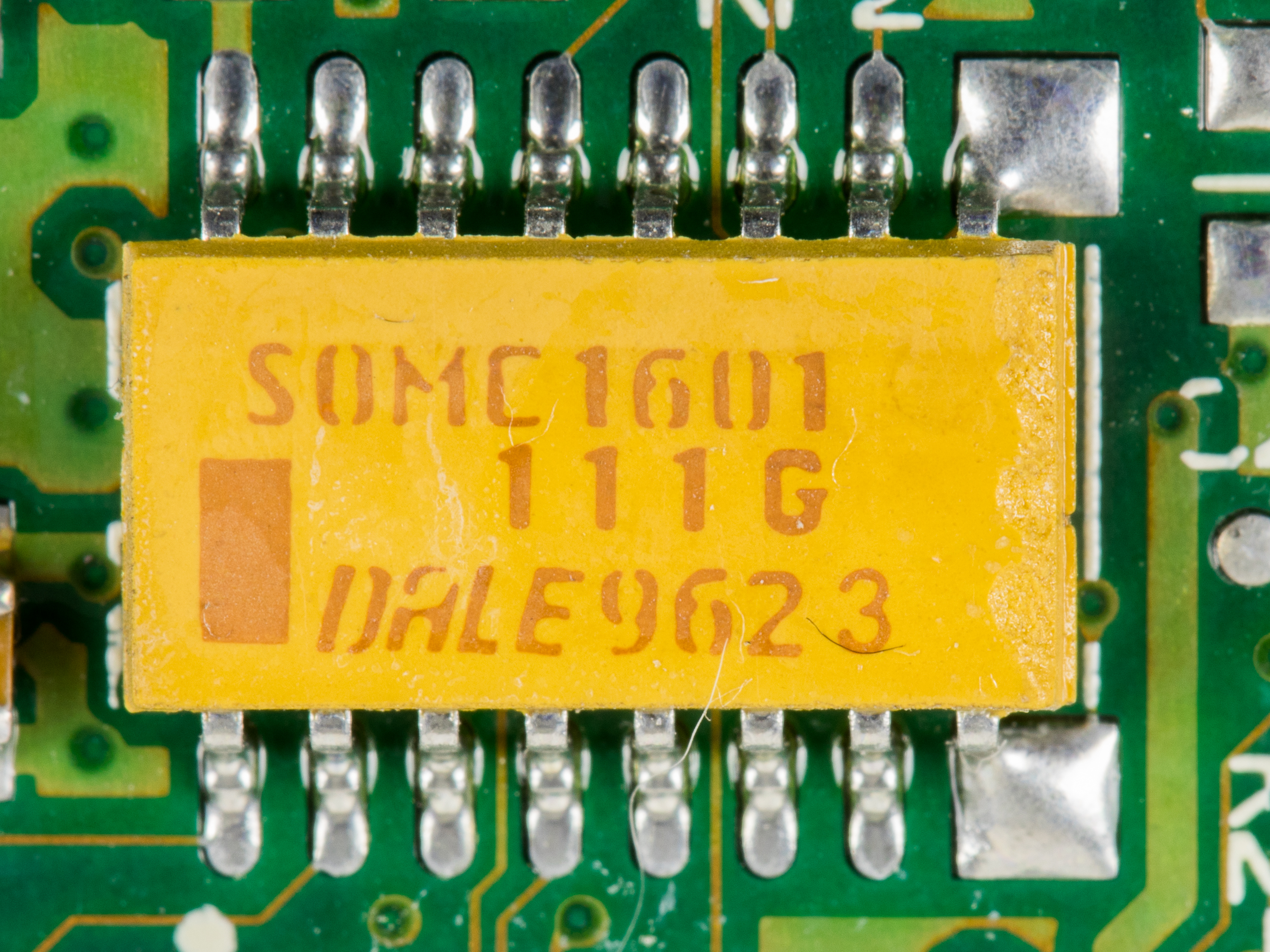
Integrated passive devices (IPDs), also known as integrated passive components (IPCs) or embedded passive components (EPC), are electronic components where resistors (R), capacitors (C), inductors (L)/coils/chokes, microstriplines, impedance matching elements, baluns or any combinations of them are integrated in the same package or on the same substrate. Sometimes integrated passives can also be called as embedded passives, and still the difference between integrated and embedded passives is technically unclear. In both cases passives are realized in between dielectric layers or on the same substrate. The earliest form of IPDs are resistor, capacitor, resistor-capacitor (RC) or resistor-capacitor-coil/inductor (RCL) networks. Passive transformers can also be realised as integrated passive devices like by putting two coils on top of each other separated by a thin dielectric layer. Sometimes diodes (PN, PIN, zener etc.) can be integrated on the same substrate with integrated passives ... [...More Info...] [...Related Items...] OR: [Wikipedia] [Google] [Baidu] |
Thick-film
Thick-film technology is used to produce electronic devices/modules such as surface mount devices modules, hybrid integrated circuits, heating elements, integrated passive devices and sensors. Main manufacturing technique is screen printing (stenciling), which in addition to use in manufacturing electronic devices can also be used for various graphic reproduction targets. It became one of the key manufacturing/miniaturisation techniques of electronic devices/modules during 1950s. Typical film thickness – manufactured with thick film manufacturing processes for electronic devices – is 0.0001 to 0.1 mm. Thick-film circuits/modules are widely used in the automotive industry, both in sensors, e.g. mixture of fuel/air, pressure sensors, engine and gearbox controls, sensor for releasing airbags, ignitors to airbags; common is that high reliability is required, often extended temperature range also along massive thermocycling of circuits without failure. Other application areas ... [...More Info...] [...Related Items...] OR: [Wikipedia] [Google] [Baidu] |
Photolithography
In integrated circuit manufacturing, photolithography or optical lithography is a general term used for techniques that use light to produce minutely patterned thin films of suitable materials over a substrate, such as a silicon wafer (electronics), wafer, to protect selected areas of it during subsequent etching, Chemical vapor deposition, deposition, or Ion implantation, implantation operations. Typically, ultraviolet light is used to transfer a geometry, geometric design from an photomask, optical mask to a photosensitivity, light-sensitive chemical (photoresist) coated on the substrate. The photoresist either breaks down or hardens where it is exposed to light. The patterned film is then created by removing the softer parts of the coating with appropriate solvents. Conventional photoresists typically consists of three components: resin, sensitizer, and solvent. Photolithography processes can be classified according to the type of light used, such as ultraviolet, deep ultrav ... [...More Info...] [...Related Items...] OR: [Wikipedia] [Google] [Baidu] |
Wafer (electronics)
In electronics, a wafer (also called a slice or substrate) is a thin slice of semiconductor, such as a crystalline silicon (c-Si), used for the fabrication of integrated circuits and, in photovoltaics, to manufacture solar cells. The wafer serves as the substrate for microelectronic devices built in and upon the wafer. It undergoes many microfabrication processes, such as doping, ion implantation, etching, thin-film deposition of various materials, and photolithographic patterning. Finally, the individual microcircuits are separated by wafer dicing and packaged as an integrated circuit. History In the semiconductor or silicon wafer industry, the term wafer appeared in the 1950s to describe a thin round slice of semiconductor material, typically germanium or silicon. Round shape comes from single-crystal ingots usually produced using the Czochralski method. Silicon wafers were first introduced in the 1940s. By 1960, silicon wafers were being manufactured in the U.S. by c ... [...More Info...] [...Related Items...] OR: [Wikipedia] [Google] [Baidu] |
Surface-mount Technology
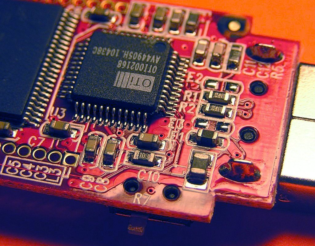
Surface-mount technology (SMT), originally called planar mounting, is a method in which the electrical components are mounted directly onto the surface of a printed circuit board (PCB). An electrical component mounted in this manner is referred to as a surface-mount device (SMD). In industry, this approach has largely replaced the through-hole technology construction method of fitting components, in large part because SMT allows for increased manufacturing automation which reduces cost and improves quality. It also allows for more components to fit on a given area of substrate. Both technologies can be used on the same board, with the through-hole technology often used for components not suitable for surface mounting such as large transformers and heat-sinked power semiconductors. An SMT component is usually smaller than its through-hole counterpart because it has either smaller leads or no leads at all. It may have short pins or leads of various styles, flat contacts, a matri ... [...More Info...] [...Related Items...] OR: [Wikipedia] [Google] [Baidu] |
Atomic Layer Deposition
Atomic layer deposition (ALD) is a thin-film deposition technique based on the sequential use of a gas-phase chemical process; it is a subclass of chemical vapour deposition. The majority of ALD reactions use two chemicals called precursors (also called "reactants"). These precursors react with the surface of a material one at a time in a sequential, self-limiting, manner. A thin film is slowly deposited through repeated exposure to separate precursors. ALD is a key process in fabricating semiconductor devices, and part of the set of tools for synthesising nanomaterials. Introduction During atomic layer deposition a film is grown on a substrate by exposing its surface to alternate gaseous species (typically referred to as precursors or reactants). In contrast to chemical vapor deposition, the precursors are never present simultaneously in the reactor, but they are inserted as a series of sequential, non-overlapping pulses. In each of these pulses the precursor molecules reac ... [...More Info...] [...Related Items...] OR: [Wikipedia] [Google] [Baidu] |
Surface Mount
Surface-mount technology (SMT), originally called planar mounting, is a method in which the electrical components are mounted directly onto the surface of a printed circuit board (PCB). An electrical component mounted in this manner is referred to as a surface-mount device (SMD). In industry, this approach has largely replaced the through-hole technology construction method of fitting components, in large part because SMT allows for increased manufacturing automation which reduces cost and improves quality. It also allows for more components to fit on a given area of substrate. Both technologies can be used on the same board, with the through-hole technology often used for components not suitable for surface mounting such as large transformers and heat-sinked power semiconductors. An SMT component is usually smaller than its through-hole counterpart because it has either smaller leads or no leads at all. It may have short pins or leads of various styles, flat contacts, a matri ... [...More Info...] [...Related Items...] OR: [Wikipedia] [Google] [Baidu] |
Electrostatic Discharge
Electrostatic discharge (ESD) is a sudden and momentary flow of electric current between two electrically charged objects caused by contact, an electrical short or dielectric breakdown. A buildup of static electricity can be caused by tribocharging or by electrostatic induction. The ESD occurs when differently-charged objects are brought close together or when the dielectric between them breaks down, often creating a visible spark. ESD can create spectacular electric sparks (lightning, with the accompanying sound of thunder, is a large-scale ESD event), but also less dramatic forms which may be neither seen nor heard, yet still be large enough to cause damage to sensitive electronic devices. Electric sparks require a field strength above approximately 40 kV/cm in air, as notably occurs in lightning strikes. Other forms of ESD include corona discharge from sharp electrodes and brush discharge from blunt electrodes. ESD can cause harmful effects of importance in industry, in ... [...More Info...] [...Related Items...] OR: [Wikipedia] [Google] [Baidu] |
Electromagnetic Interference
Electromagnetic interference (EMI), also called radio-frequency interference (RFI) when in the radio frequency spectrum, is a disturbance generated by an external source that affects an electrical circuit by electromagnetic induction, electrostatic coupling, or conduction. The disturbance may degrade the performance of the circuit or even stop it from functioning. In the case of a data path, these effects can range from an increase in error rate to a total loss of the data. Both man-made and natural sources generate changing electrical currents and voltages that can cause EMI: ignition systems, cellular network of mobile phones, lightning, solar flares, and auroras (northern/southern lights). EMI frequently affects AM radios. It can also affect mobile phones, FM radios, and televisions, as well as observations for radio astronomy and atmospheric science. EMI can be used intentionally for radio jamming, as in electronic warfare. History Since the earliest days o ... [...More Info...] [...Related Items...] OR: [Wikipedia] [Google] [Baidu] |
Interposer
An interposer is an electrical interface routing between one socket or connection to another. The purpose of an interposer is to spread a connection to a wider pitch or to reroute a connection to a different connection. Interposer comes from the Latin word "interpōnere", meaning "to put between". They are often used in BGA packages, multi-chip modules and high bandwidth memory. A common example of an interposer is an integrated circuit die to BGA, such as in the Pentium II. This is done through various substrates, both rigid and flexible, most commonly FR4 for rigid, and polyimide for flexible. Silicon and glass are also evaluated as an integration method. Interposer stacks are also a widely accepted, cost-effective alternative to 3D ICs. There are already several products with interposer technology in the market, notably the AMD Fiji/Fury GPU, and the Xilinx Virtex-7 FPGA. In 2016, CEA Leti demonstrated their second generation 3D-NoC technology which combines small ... [...More Info...] [...Related Items...] OR: [Wikipedia] [Google] [Baidu] |
Ball Grid Array
A ball grid array (BGA) is a type of surface-mount packaging (a chip carrier) used for integrated circuits. BGA packages are used to permanently mount devices such as microprocessors. A BGA can provide more interconnection pins than can be put on a dual in-line or flat package. The whole bottom surface of the device can be used, instead of just the perimeter. The traces connecting the package's leads to the wires or balls which connect the die to package are also on average shorter than with a perimeter-only type, leading to better performance at high speeds. BGAs were introduced in the 1990s and became popular by 2001. Soldering of BGA devices requires precise control and is usually done by automated processes such as in computer-controlled automatic reflow ovens. Description The BGA is descended from the pin grid array (PGA), which is a package with one face covered (or partly covered) with pins in a grid pattern which, in operation, conduct electrical signals between ... [...More Info...] [...Related Items...] OR: [Wikipedia] [Google] [Baidu] |
Integrated Circuits
An integrated circuit or monolithic integrated circuit (also referred to as an IC, a chip, or a microchip) is a set of electronic circuits on one small flat piece (or "chip") of semiconductor material, usually silicon. Transistor count, Large numbers of tiny MOSFETs (metal–oxide–semiconductor field-effect transistors) integrate into a small chip. This results in circuits that are orders of magnitude smaller, faster, and less expensive than those constructed of discrete electronic components. The IC's mass production capability, reliability, and building-block approach to integrated circuit design has ensured the rapid adoption of standardized ICs in place of designs using discrete transistors. ICs are now used in virtually all electronic equipment and have revolutionized the world of electronics. Computers, mobile phones and other home appliances are now inextricable parts of the structure of modern societies, made possible by the small size and low cost of ICs such as mode ... [...More Info...] [...Related Items...] OR: [Wikipedia] [Google] [Baidu] |


.jpg)