|
Contact Pad
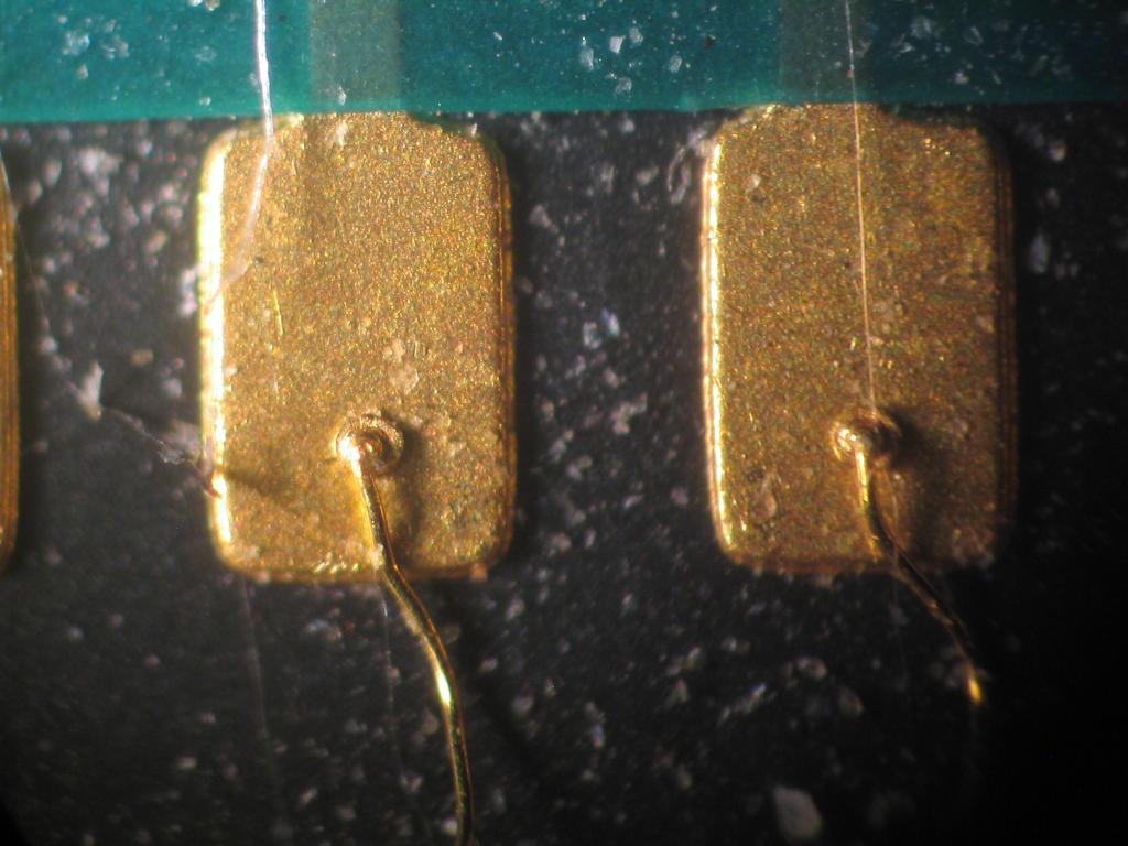
Contact pads or bond pads are designated surface areas of a printed circuit board (PCB) or die of an integrated circuit. Possibilities to contact to pads include soldering, wirebonding, flip chip Flip chip, also known as controlled collapse chip connection or its abbreviation, C4, is a method for interconnecting dies such as semiconductor devices, IC chips, integrated passive devices and microelectromechanical systems (MEMS), to exter ... mounting, or probe needles. Further reading *Kraig Mitzner, ''Complete PCB Design Using OrCAD Capture and PCB Editor'', Newnes, 2009 . *Jing Li, ''Evaluation and Improvement of the Robustness of a PCB Pad in a Lead-free Environment'', ProQuest, 2007 . *Deborah Lea, Fredirikus Jonck, Christopher Hunt, ''Solderability Measurements of PCB Pad Finishes and Geometries'', National Physical Laboratory, 2001 . Electronic engineering Printed circuit board manufacturing {{Electronics-stub ... [...More Info...] [...Related Items...] OR: [Wikipedia] [Google] [Baidu] |
Printed Circuit Board
A printed circuit board (PCB; also printed wiring board or PWB) is a medium used in Electrical engineering, electrical and electronic engineering to connect electronic components to one another in a controlled manner. It takes the form of a Lamination, laminated sandwich structure of conductive and insulating layers: each of the conductive layers is designed with an artwork pattern of traces, planes and other features (similar to wires on a flat surface) Chemical milling, etched from one or more sheet layers of copper Lamination, laminated onto and/or between sheet layers of a Insulator (electricity), non-conductive substrate. Electrical components may be fixed to conductive pads on the outer layers in the shape designed to accept the component's terminals, generally by means of soldering, to both electrically connect and mechanically fasten them to it. Another manufacturing process adds Via (electronics), vias: plated-through holes that allow interconnections between layers. ... [...More Info...] [...Related Items...] OR: [Wikipedia] [Google] [Baidu] |
Die (integrated Circuit)
A die, in the context of integrated circuits, is a small block of semiconducting material on which a given functional circuit is fabricated. Typically, integrated circuits are produced in large batches on a single wafer of electronic-grade silicon (EGS) or other semiconductor (such as GaAs) through processes such as photolithography. The wafer is cut (diced) into many pieces, each containing one copy of the circuit. Each of these pieces is called a die. There are three commonly used plural forms: ''dice'', ''dies'' and ''die''. To simplify handling and integration onto a printed circuit board, most dies are packaged in various forms. Manufacturing process Most dies are composed of silicon and used for integrated circuits. The process begins with the production of monocrystalline silicon ingots. These ingots are then sliced into disks with a diameter of up to 300 mm. [...More Info...] [...Related Items...] OR: [Wikipedia] [Google] [Baidu] |
Integrated Circuit
An integrated circuit or monolithic integrated circuit (also referred to as an IC, a chip, or a microchip) is a set of electronic circuits on one small flat piece (or "chip") of semiconductor material, usually silicon. Large numbers of tiny MOSFETs (metal–oxide–semiconductor field-effect transistors) integrate into a small chip. This results in circuits that are orders of magnitude smaller, faster, and less expensive than those constructed of discrete electronic components. The IC's mass production capability, reliability, and building-block approach to integrated circuit design has ensured the rapid adoption of standardized ICs in place of designs using discrete transistors. ICs are now used in virtually all electronic equipment and have revolutionized the world of electronics. Computers, mobile phones and other home appliances are now inextricable parts of the structure of modern societies, made possible by the small size and low cost of ICs such as modern computer ... [...More Info...] [...Related Items...] OR: [Wikipedia] [Google] [Baidu] |
Solder
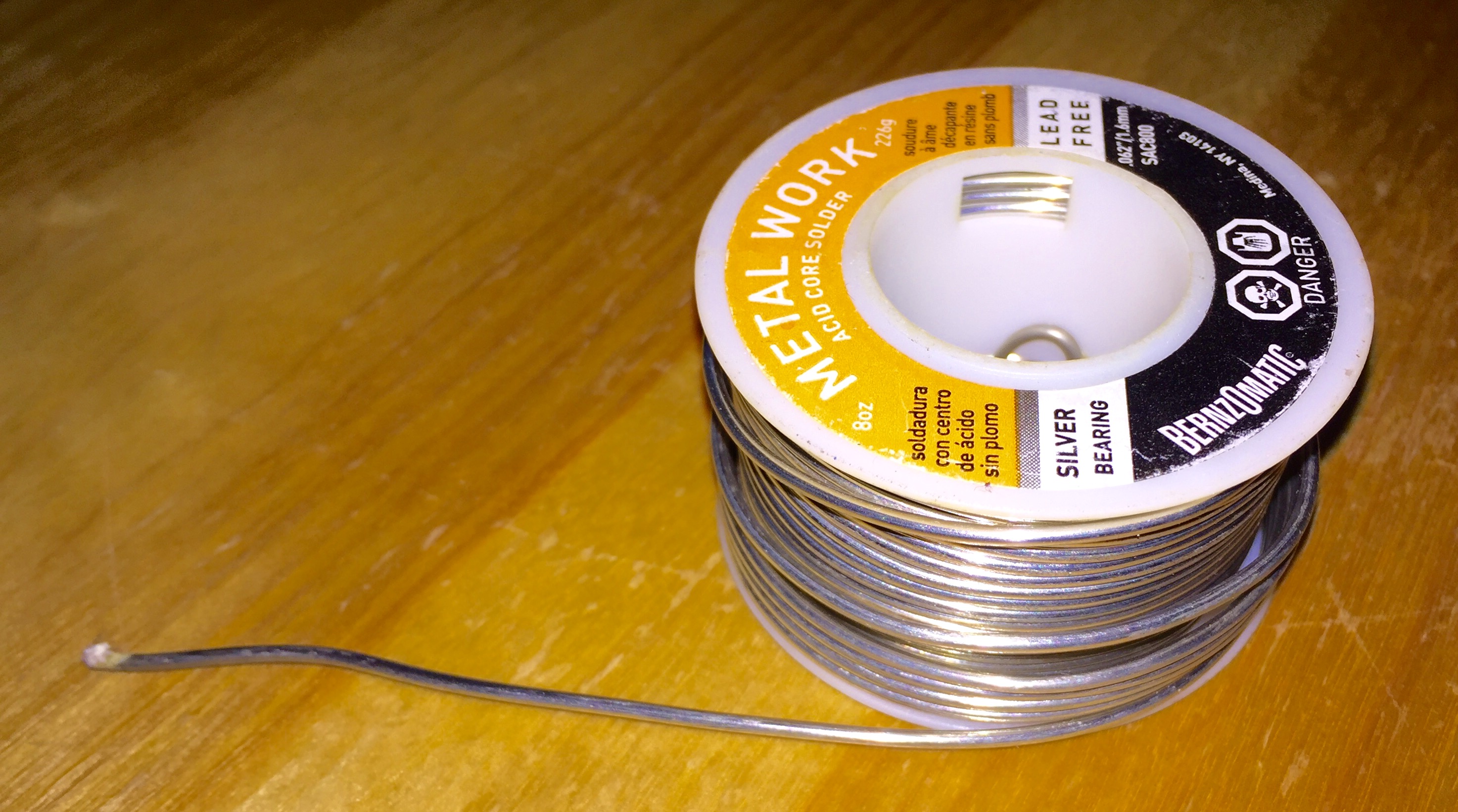
Solder (; NA: ) is a fusible metal alloy used to create a permanent bond between metal workpieces. Solder is melted in order to wet the parts of the joint, where it adheres to and connects the pieces after cooling. Metals or alloys suitable for use as solder should have a lower melting point than the pieces to be joined. The solder should also be resistant to oxidative and corrosive effects that would degrade the joint over time. Solder used in making electrical connections also needs to have favorable electrical characteristics. Soft solder typically has a melting point range of , and is commonly used in electronics, plumbing, and sheet metal work. Alloys that melt between are the most commonly used. Soldering performed using alloys with a melting point above is called "hard soldering", "silver soldering", or brazing. In specific proportions, some alloys are eutectic — that is, the alloy's melting point is the lowest possible for a mixture of those components, and co ... [...More Info...] [...Related Items...] OR: [Wikipedia] [Google] [Baidu] |
Wire Bonding
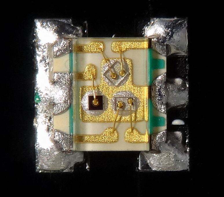
Wire bonding is the method of making interconnections between an integrated circuit (IC) or other semiconductor device and its packaging during semiconductor device fabrication. Although less common, wire bonding can be used to connect an IC to other electronics or to connect from one printed circuit board (PCB) to another. Wire bonding is generally considered the most cost-effective and flexible interconnect technology and is used to assemble the vast majority of semiconductor packages. Wire bonding can be used at frequencies above 100 GHz. [...More Info...] [...Related Items...] OR: [Wikipedia] [Google] [Baidu] |
Flip Chip
Flip chip, also known as controlled collapse chip connection or its abbreviation, C4, is a method for interconnecting dies such as semiconductor devices, IC chips, integrated passive devices and microelectromechanical systems (MEMS), to external circuitry with solder bumps that have been deposited onto the chip pads. The technique was developed by General Electric's Light Military Electronics Department, Utica, New York. The solder bumps are deposited on the chip pads on the top side of the wafer during the final wafer processing step. In order to mount the chip to external circuitry (e.g., a circuit board or another chip or wafer), it is flipped over so that its top side faces down, and aligned so that its pads align with matching pads on the external circuit, and then the solder is reflowed to complete the interconnect. This is in contrast to wire bonding, in which the chip is mounted upright and fine wires are welded onto the chip pads and lead frame contacts to interconnect t ... [...More Info...] [...Related Items...] OR: [Wikipedia] [Google] [Baidu] |
Probe Card
A probe card is an interface between an electronic test system and a semiconductor wafer. Typically the probe card is mechanically docked to a prober and electrically connected to a tester. Its purpose is to provide an electrical path between the test system and the circuits on the wafer, thereby permitting the testing and validation of the circuits at the wafer level, usually before they are diced and packaged. It consists, normally, of a printed circuit board (PCB) and some form of contact elements, usually metallic, but possibly of other materials as well. A semiconductor manufacturer will typically require a new probe card for each new device wafer and for device shrinks (when the manufacturer reduces the size of the device while keeping its functionality) because the probe card is effectively a custom connector that takes the universal pattern of a given tester and translates the signals to connect to electrical pads on the wafer. For testing of DRAM and FLASH memory dev ... [...More Info...] [...Related Items...] OR: [Wikipedia] [Google] [Baidu] |
Electronic Engineering
Electronics engineering is a sub-discipline of electrical engineering which emerged in the early 20th century and is distinguished by the additional use of active components such as semiconductor devices to amplify and control electric current flow. Previously electrical engineering only used passive devices such as mechanical switches, resistors, inductors and capacitors. It covers fields such as: analog electronics, digital electronics, consumer electronics, embedded systems and power electronics. It is also involved in many related fields, for example solid-state physics, radio engineering, telecommunications, control systems, signal processing, systems engineering, computer engineering, instrumentation engineering, electric power control, robotics. The Institute of Electrical and Electronics Engineers (IEEE) is one of the most important professional bodies for electronics engineers in the US; the equivalent body in the UK is the Institution of Engineering and Technology ... [...More Info...] [...Related Items...] OR: [Wikipedia] [Google] [Baidu] |


.jpg)

