|
Back End Of Line
The back end of line (BEOL) is the second portion of IC fabrication where the individual devices (transistors, capacitors, resistors, etc.) get interconnected with wiring on the wafer, the metalization layer. Common metals are copper and aluminum. BEOL generally begins when the first layer of metal is deposited on the wafer. BEOL includes contacts, insulating layers (dielectrics), metal levels, and bonding sites for chip-to-package connections. After the last FEOL step, there is a wafer with isolated transistors (without any wires). In BEOL part of fabrication stage contacts (pads), interconnect wires, vias and dielectric structures are formed. For modern IC process, more than 10 metal layers can be added in the BEOL. Steps of the BEOL: # Silicidation of source and drain regions and the polysilicon region. # Adding a dielectric (first, lower layer is pre-metal dielectric (PMD) – to isolate metal from silicon and polysilicon), CMP processing it # Make holes in PMD, make a ... [...More Info...] [...Related Items...] OR: [Wikipedia] [Google] [Baidu] |
Chemical-mechanical Planarization
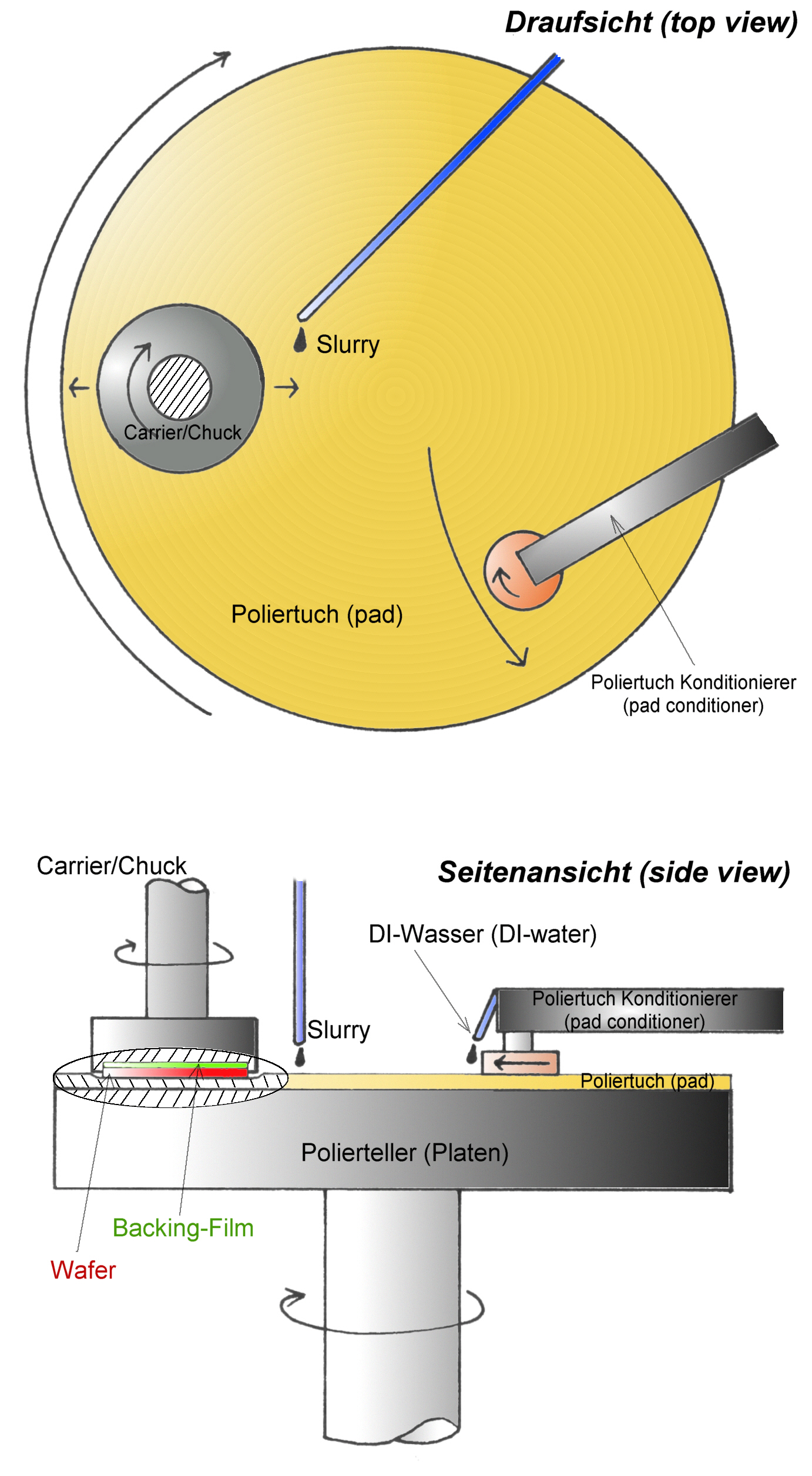
Chemical mechanical polishing (CMP) or planarization is a process of smoothing surfaces with the combination of chemical and mechanical forces. It can be thought of as a hybrid of chemical etching and free abrasive polishing. Description The process uses an abrasive and corrosive chemical slurry (commonly a colloid) in conjunction with a polishing pad and retaining ring, typically of a greater diameter than the wafer. The pad and wafer are pressed together by a dynamic polishing head and held in place by a plastic retaining ring. The dynamic polishing head is rotated with different axes of rotation (i.e., not concentric). This removes material and tends to even out any irregular topography, making the wafer flat or planar. This may be necessary to set up the wafer for the formation of additional circuit elements. For example, CMP can bring the entire surface within the depth of field of a photolithography system, or selectively remove material based on its position. Typical depth-o ... [...More Info...] [...Related Items...] OR: [Wikipedia] [Google] [Baidu] |
Integrated Circuit
An integrated circuit or monolithic integrated circuit (also referred to as an IC, a chip, or a microchip) is a set of electronic circuits on one small flat piece (or "chip") of semiconductor material, usually silicon. Large numbers of tiny MOSFETs (metal–oxide–semiconductor field-effect transistors) integrate into a small chip. This results in circuits that are orders of magnitude smaller, faster, and less expensive than those constructed of discrete electronic components. The IC's mass production capability, reliability, and building-block approach to integrated circuit design has ensured the rapid adoption of standardized ICs in place of designs using discrete transistors. ICs are now used in virtually all electronic equipment and have revolutionized the world of electronics. Computers, mobile phones and other home appliances are now inextricable parts of the structure of modern societies, made possible by the small size and low cost of ICs such as modern computer ... [...More Info...] [...Related Items...] OR: [Wikipedia] [Google] [Baidu] |
Front End Of Line
The front-end-of-line (FEOL) is the first portion of IC fabrication where the individual components (transistors, capacitors, resistors, etc.) are patterned in the semiconductor. FEOL generally covers everything up to (but not including) the deposition of metal interconnect layers. For the CMOS process, FEOL contains all fabrication steps needed to form isolated CMOS elements: # Selecting the type of wafer to be used; Chemical-mechanical planarization and cleaning of the wafer. # Shallow trench isolation (STI) (or LOCOS in early processes, with feature size > 0.25 μm) # Well formation # Gate module formation # Source and drain module formation See also * Back end of line *Integrated circuit An integrated circuit or monolithic integrated circuit (also referred to as an IC, a chip, or a microchip) is a set of electronic circuits on one small flat piece (or "chip") of semiconductor material, usually silicon. Large numbers of tiny ... References Further reading *" ... [...More Info...] [...Related Items...] OR: [Wikipedia] [Google] [Baidu] |
Integrated Circuit Packaging
In electronics manufacturing, integrated circuit packaging is the final stage of semiconductor device fabrication, in which the block of semiconductor material is encapsulated in a supporting case that prevents physical damage and corrosion. The case, known as a " package", supports the electrical contacts which connect the device to a circuit board. In the integrated circuit industry, the process is often referred to as packaging. Other names include semiconductor device assembly, assembly, encapsulation or sealing. The packaging stage is followed by testing of the integrated circuit. The term is sometimes confused with electronic packaging, which is the mounting and interconnecting of integrated circuits (and other components) onto printed-circuit boards. Design considerations Electrical The current-carrying traces that run out of the die, through the package, and into the printed circuit board (PCB) have very different electrical properties compared to on-chip signal ... [...More Info...] [...Related Items...] OR: [Wikipedia] [Google] [Baidu] |
Die Preparation
Die preparation is a step of semiconductor device fabrication during which a wafer is prepared for IC packaging and IC testing. The process of die preparation typically consists of two steps: wafer mounting and wafer dicing. Wafer mounting Wafer mounting is a step that is performed during the die preparation of a wafer as part of the process of semiconductor fabrication. During this step, the wafer is mounted on a plastic tape that is attached to a ring. Wafer mounting is performed right before the wafer is cut into separate dies. The adhesive film upon which the wafer is mounted ensures that the individual dies remain firmly in place during 'dicing', as the process of cutting the wafer is called. The picture on the right shows a 300 mm wafer after it was mounted and diced. The blue plastic is the adhesive tape. The wafer is the round disc in the middle. In this case, a large number of dies were already removed. Semiconductor-die cutting In the manufacturing of micro-elect ... [...More Info...] [...Related Items...] OR: [Wikipedia] [Google] [Baidu] |
Wafer Backgrinding
Wafer backgrinding is a semiconductor device fabrication step during which wafer thickness is reduced to allow stacking and high-density packaging of integrated circuits (IC). ICs are produced on semiconductor wafers that undergo a multitude of processing steps. The silicon wafers predominantly used today have diameters of 200 and 300 mm. They are roughly 750 μm thick to ensure a minimum of mechanical stability and to avoid warping during high-temperature processing steps. Smartcards, USB memory sticks, smartphones, handheld music players, and other ultra-compact electronic products would not be feasible in their present form without minimizing the size of their various components along all dimensions. The backside of the wafers are thus ground prior to wafer dicing (separation of the individual microchips). Wafers thinned down to 75 to 50 μm are common today. [...More Info...] [...Related Items...] OR: [Wikipedia] [Google] [Baidu] |
Wafer Testing
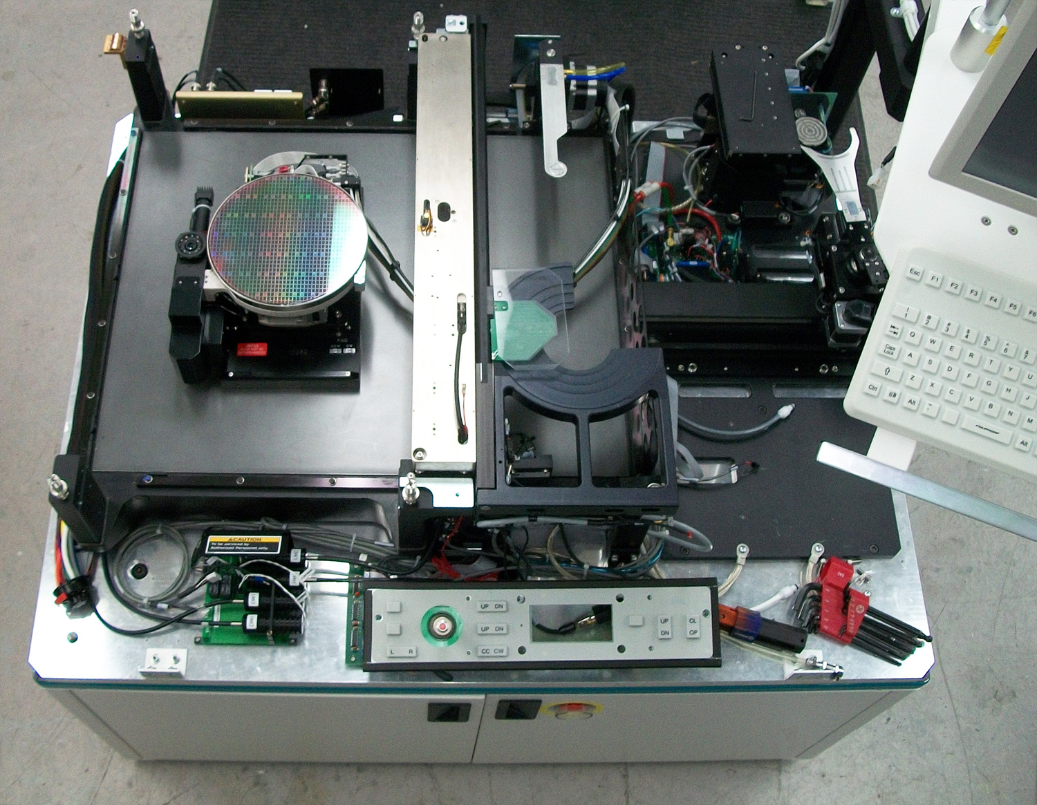
Wafer testing is a step performed during semiconductor device fabrication after BEOL process is finished. During this step, performed before a wafer is sent to die preparation, all individual integrated circuits that are present on the wafer are tested for functional defects by applying special test patterns to them. The wafer testing is performed by a piece of test equipment called a wafer prober. The process of wafer testing can be referred to in several ways: Wafer Final Test (WFT), Electronic Die Sort (EDS) and Circuit Probe (CP) are probably the most common. Wafer prober A wafer prober is a machine used for integrated circuits verification against designed functionality. It's either manual or automatic test equipment. For electrical testing a set of microscopic contacts or probes called a probe card are held in place whilst the wafer, vacuum-mounted on a wafer chuck, is moved into electrical contact. When a die (or array of dice) have been electrically tested the prober mo ... [...More Info...] [...Related Items...] OR: [Wikipedia] [Google] [Baidu] |
Chemical Vapor Deposition
Chemical vapor deposition (CVD) is a vacuum deposition method used to produce high quality, and high-performance, solid materials. The process is often used in the semiconductor industry to produce thin films. In typical CVD, the wafer (substrate) is exposed to one or more volatile precursors, which react and/or decompose on the substrate surface to produce the desired deposit. Frequently, volatile by-products are also produced, which are removed by gas flow through the reaction chamber. Microfabrication processes widely use CVD to deposit materials in various forms, including: monocrystalline, polycrystalline, amorphous, and epitaxial. These materials include: silicon ( dioxide, carbide, nitride, oxynitride), carbon (fiber, nanofibers, nanotubes, diamond and graphene), fluorocarbons, filaments, tungsten, titanium nitride and various high-κ dielectrics. The term ''chemical vapour deposition'' was coined 1960 by ''John M. Blocher, Jr.'' who intended to differentiate ''chemic ... [...More Info...] [...Related Items...] OR: [Wikipedia] [Google] [Baidu] |
CMOS Fabrication Process
Complementary metal–oxide–semiconductor (CMOS, pronounced "sea-moss", ) is a type of metal–oxide–semiconductor field-effect transistor (MOSFET) fabrication process that uses complementary and symmetrical pairs of p-type and n-type MOSFETs for logic functions. CMOS technology is used for constructing integrated circuit (IC) chips, including microprocessors, microcontrollers, memory chips (including CMOS BIOS), and other digital logic circuits. CMOS technology is also used for analog circuits such as image sensors (CMOS sensors), data converters, RF circuits (RF CMOS), and highly integrated transceivers for many types of communication. The CMOS process was originally conceived by Frank Wanlass at Fairchild Semiconductor and presented by Wanlass and Chih-Tang Sah at the International Solid-State Circuits Conference in 1963. Wanlass later filed US patent 3,356,858 for CMOS circuitry and it was granted in 1967. commercialized the technology with the trademark "COS-MOS" ... [...More Info...] [...Related Items...] OR: [Wikipedia] [Google] [Baidu] |

.jpg)
