|
Work Function
In solid-state physics, the work function (sometimes spelt workfunction) is the minimum thermodynamic work (i.e., energy) needed to remove an electron from a solid to a point in the vacuum immediately outside the solid surface. Here "immediately" means that the final electron position is far from the surface on the atomic scale, but still too close to the solid to be influenced by ambient electric fields in the vacuum. The work function is not a characteristic of a bulk material, but rather a property of the surface of the material (depending on crystal face and contamination). Definition The work function for a given surface is defined by the difference :W = -e\phi - E_, where is the charge of an electron, is the electrostatic potential in the vacuum nearby the surface, and is the Fermi level (electrochemical potential of electrons) inside the material. The term is the energy of an electron at rest in the vacuum nearby the surface. In practice, one directly controls by ... [...More Info...] [...Related Items...] OR: [Wikipedia] [Google] [Baidu] |
Solid-state Physics
Solid-state physics is the study of rigid matter, or solids, through methods such as quantum mechanics, crystallography, electromagnetism, and metallurgy. It is the largest branch of condensed matter physics. Solid-state physics studies how the large-scale properties of solid materials result from their atomic-scale properties. Thus, solid-state physics forms a theoretical basis of materials science. It also has direct applications, for example in the technology of transistors and semiconductors. Background Solid materials are formed from densely packed atoms, which interact intensely. These interactions produce the mechanical (e.g. hardness and Elasticity (physics), elasticity), Heat conduction, thermal, Electrical conduction, electrical, Magnetism, magnetic and Crystal optics, optical properties of solids. Depending on the material involved and the conditions in which it was formed, the atoms may be arranged in a regular, geometric pattern (crystal, crystalline solids, ... [...More Info...] [...Related Items...] OR: [Wikipedia] [Google] [Baidu] |
Hot Cathode
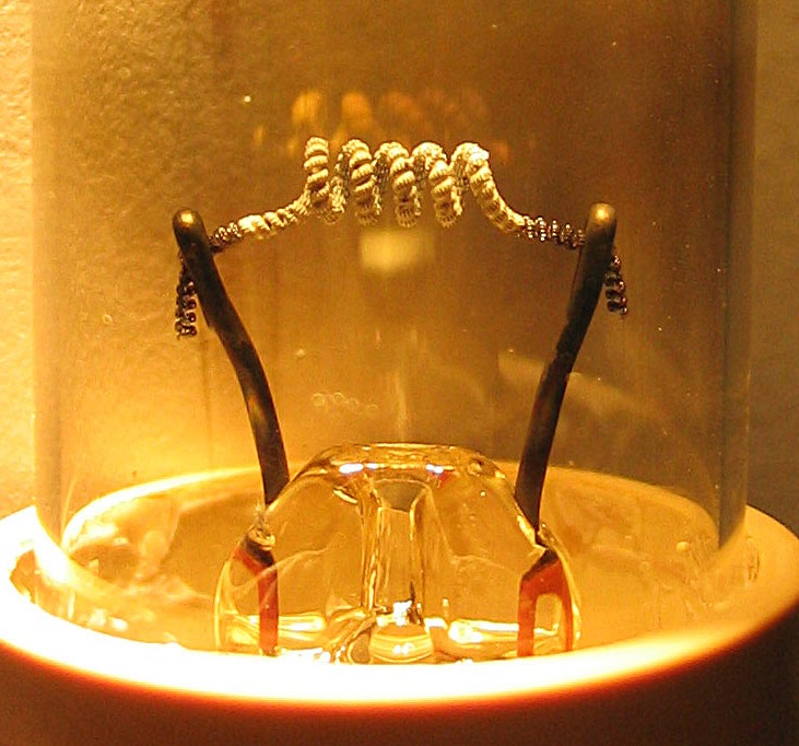
In vacuum tubes and gas-filled tubes, a hot cathode or thermionic cathode is a cathode electrode which is heated to make it emit electrons due to thermionic emission. This is in contrast to a cold cathode, which does not have a heating element. The heating element is usually an electrical filament heated by a separate electric current passing through it. Hot cathodes typically achieve much higher power density than cold cathodes, emitting significantly more electrons from the same surface area. Cold cathodes rely on field electron emission or secondary electron emission from positive ion bombardment, and do not require heating. There are two types of hot cathode. In a ''directly heated cathode'', the filament is the cathode and emits the electrons. In an ''indirectly heated cathode'', the filament or ''heater'' heats a separate metal cathode electrode which emits the electrons. From the 1920s to the 1960s, a wide variety of electronic devices used hot-cathode vacuum tubes. T ... [...More Info...] [...Related Items...] OR: [Wikipedia] [Google] [Baidu] |
Surface Charge
Surface charge is a two-dimensional surface with non-zero electric charge. These electric charges are constrained on this 2-D surface, and surface charge density, measured in coulombs per square meter (C•m−2), is used to describe the charge distribution on the surface. The electric potential is continuous across a surface charge and the electric field is discontinuous, but not infinite; this is unless the surface charge consists of a dipole layer. In comparison, the potential and electric field both diverge at any point charge or linear charge. In physics, at equilibrium, an ideal conductor has no charge on its interior; instead, the entirety of the charge of the conductor resides on the surface. However, this only applies to the ideal case of infinite electrical conductivity; The majority of the charge of an actual conductor resides within the skin depth of the conductor's surface. For dielectric materials, upon the application of an external electric field, the positive charg ... [...More Info...] [...Related Items...] OR: [Wikipedia] [Google] [Baidu] |
Contact Electrification
Contact electrification is a phrase that describes a phenomenon whereby surfaces become electrically charged, via a number of possible mechanisms, when two or more objects come within close proximity of one another. When two objects are "touched" together, sometimes the objects become spontaneously charged. One object may develop a net negative charge, while the other develops an equal and opposite positive charge. This effect may be caused by various physical processes – triboelectricity, the Volta effect, differing work functions of metals, and others which are collective referred to as contact electrification. The contact electrification phenomenon allowed the construction of so-called 'frictional' electrostatic generators such as Ramsden's or Winter's machines, but it also led directly to the development of useful devices such as Battery (electricity), batteries, fuel cells, electroplating, thermocouples. Contact between materials is responsible for such modern electrical te ... [...More Info...] [...Related Items...] OR: [Wikipedia] [Google] [Baidu] |
Gravity Probe B
Gravity Probe B (GP-B) was a satellite-based experiment to test two unverified predictions of general relativity: the geodetic effect and frame-dragging. This was to be accomplished by measuring, very precisely, tiny changes in the direction of spin of four gyroscopes contained in an Earth-orbiting satellite at of altitude, crossing directly over the poles. The satellite was launched on 20 April 2004 on a Delta II rocket. The spaceflight phase lasted until 2005; Its aim was to measure spacetime curvature near Earth, and thereby the stress–energy tensor (which is related to the distribution and the motion of matter in space) in and near Earth. This provided a test of general relativity, gravitomagnetism and related models. The principal investigator was Francis Everitt. Initial results confirmed the expected geodetic effect to an accuracy of about 1%. The expected frame-dragging effect was similar in magnitude to the current noise level (the noise being dominated by initially ... [...More Info...] [...Related Items...] OR: [Wikipedia] [Google] [Baidu] |
Casimir Force
In quantum field theory, the Casimir effect is a physical force acting on the macroscopic boundaries of a confined space which arises from the quantum fluctuations of the field. It is named after the Dutch physicist Hendrik Casimir, who predicted the effect for electromagnetic systems in 1948. In the same year, Casimir together with Dirk Polder described a similar effect experienced by a neutral atom in the vicinity of a macroscopic interface which is referred to as the Casimir–Polder force. Their result is a generalization of the London–van der Waals force and includes retardation due to the finite speed of light. Since the fundamental principles leading to the London–van der Waals force, the Casimir and the Casimir–Polder force, respectively, can be formulated on the same footing, the distinction in nomenclature nowadays serves a historical purpose mostly and usually refers to the different physical setups. It was not until 1997 that a direct experiment by S. Lamorea ... [...More Info...] [...Related Items...] OR: [Wikipedia] [Google] [Baidu] |
Herbert Kroemer
Herbert Kroemer (; born August 25, 1928) is a German-American physicist who, along with Zhores Alferov, received the Nobel Prize in Physics in 2000 for "developing semiconductor heterostructures used in high-speed- and opto-electronics". Kroemer is professor emeritus of electrical and computer engineering at the University of California, Santa Barbara, having received his Ph.D. in theoretical physics in 1952 from the University of Göttingen, Germany, with a dissertation on hot electron effects in the then-new transistor. His research into transistors was a stepping stone to the later development of mobile phone technologies. Career Kroemer worked in a number of research laboratories in Germany and the United States and taught electrical engineering at the University of Colorado from 1968 to 1976. He joined the UCSB faculty in 1976, focusing its semiconductor research program on the emerging compound semiconductor technology rather than on mainstream silicon technology. Along with ... [...More Info...] [...Related Items...] OR: [Wikipedia] [Google] [Baidu] |
Anderson's Rule
Anderson's rule is used for the construction of energy band diagrams of the heterojunction between two semiconductor materials. Anderson's rule states that when constructing an energy band diagram, the vacuum levels of the two semiconductors on either side of the heterojunction should be aligned (at the same energy). It is also referred to as the electron affinity rule, and is closely related to the Schottky–Mott rule for metal–semiconductor junctions. Anderson's rule was first described by R. L. Anderson in 1960. Constructing energy band diagrams Once the vacuum levels are aligned it is possible to use the electron affinity and band gap values for each semiconductor to calculate the conduction band and valence band offsets. The electron affinity (usually given by the symbol \chi in solid state physics) gives the energy difference between the lower edge of the conduction band and the vacuum level of the semiconductor. The band gap (usually given the symbol E_) gives the ... [...More Info...] [...Related Items...] OR: [Wikipedia] [Google] [Baidu] |
Heterojunction
A heterojunction is an interface between two layers or regions of dissimilar semiconductors. These semiconducting materials have unequal band gaps as opposed to a homojunction. It is often advantageous to engineer the electronic energy bands in many solid-state device applications, including semiconductor lasers, solar cells and transistors. The combination of multiple heterojunctions together in a device is called a heterostructure, although the two terms are commonly used interchangeably. The requirement that each material be a semiconductor with unequal band gaps is somewhat loose, especially on small length scales, where electronic properties depend on spatial properties. A more modern definition of heterojunction is the interface between any two solid-state materials, including crystalline and amorphous structures of metallic, insulating, fast ion conductor and semiconducting materials. Manufacture and applications Heterojunction manufacturing generally requires the use of mo ... [...More Info...] [...Related Items...] OR: [Wikipedia] [Google] [Baidu] |
Schottky Barrier
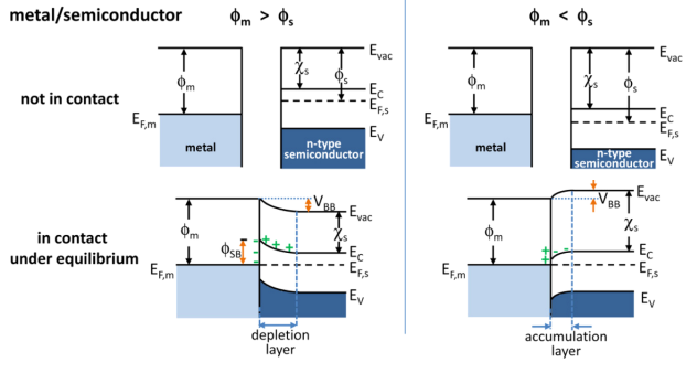
A Schottky barrier, named after Walter H. Schottky, is a potential energy barrier for electrons formed at a metal–semiconductor junction. Schottky barriers have rectifying characteristics, suitable for use as a diode. One of the primary characteristics of a Schottky barrier is the Schottky barrier height, denoted by ΦB (see figure). The value of ΦB depends on the combination of metal and semiconductor. Not all metal–semiconductor junctions form a rectifying Schottky barrier; a metal–semiconductor junction that conducts current in both directions without rectification, perhaps due to its Schottky barrier being too low, is called an ohmic contact. Physics of formation When a metal is put in direct contact with a semiconductor, a so called Schottky barrier can be formed, leading to a rectifying behavior of the electrical contact. This happens both when the semiconductor is n-type and its work function is smaller than the work function of the metal, and when the semic ... [...More Info...] [...Related Items...] OR: [Wikipedia] [Google] [Baidu] |
Band Bending
In solid-state physics, band bending refers to the process in which the electronic band structure in a material curves up or down near a junction or interface. It does not involve any physical (spatial) bending. When the electrochemical potential of the free charge carriers around an interface of a semiconductor is dissimilar, charge carriers are transferred between the two materials until an equilibrium state is reached whereby the potential difference vanishes. The band bending concept was first developed in 1938 when Mott, Davidov and Schottky all published theories of the rectifying effect of metal-semiconductor contacts. The use of semiconductor junctions sparked the computer revolution in 1990. Devices such as the diode, the transistor, the photocell and many more still play an important role in technology. Qualitative description Band bending can be induced by several types of contact. In this section metal-semiconductor contact, surface state, applied bias and adsorption ... [...More Info...] [...Related Items...] OR: [Wikipedia] [Google] [Baidu] |


